Note : Les descriptions sont présentées dans la langue officielle dans laquelle elles ont été soumises.
: 1:
q~he, p~ ~~~tes tG.-4~~e~ ~r ~eas~-~;g
flo~ to~~;c~r¢~t ~o~ opera~ 3uch a de~
Our publ~hed ~ pe~ P~ten~ Appl~ t~ ~er OZ3g7~3
de~cr~be~ ~ flow ~e~sI~g de~lce ~ the for~ oZ ~ trate of
sYmlcollductor ~oate~ abric~ted ~ith a ml~ro-ff~g~r~eerelll
cant1ever besm~ It ~cludes ~ mean~ of 8enB~ng ~ ehar~cter~8t1c
of the be~m whic~ ~8 ind~catlve o fluid flow relative to 'che
beam. Thl5 device ha~ ted ra~e of flo~ r~te~ ~psble o
bei~g mea~u~ed~ ~nd in order to co~er ~ wide ~an~e of f~ow r~tes,
~eve~al ~uch de~ioe~ ~ith different d~men3ion8 mu8t be
Incorporated on th~ 6aDI~ dil~CO~ chlp. Further~ore~ to enable
mea~ure~e~ of lo~ flow r~te~g the cantilever beam ~UEt be th~
and thi~ c~n leat ~o p~oble~ wit~ ~tre~ cau~ the beam to
bend. Anothe~ dl~ad~a~ta~e o~ t~1~ lQve~t~on ~6 that i~ th~
lS preferred capacit~noe variatio~ me~sur~me~t is l~sed to detenmine
the respo~e'of ~e c~atilev~r ~e~m to ~1uid flo~, it iS nece~fiary
that tSe 1u1d den8iq be as~umed con&ta~ Th1~ e~able~ t~
deflect~o~ o~ ~he c~nti1ever be~m to be coasider~d depende~t on
the fluid ~eloc~ty and l~depe~de~t of fluld ma6a. I~ practice,
the den~ity of the f1u~d will not be coD6tan~ ~nd ~ ~eans of
compen~ ng for c~ge~ ~ fluid d;e1ec~r~c c~n~tant would be
requi~e~.
It ia thu~ a~ object of the present l~e~tlo~ to prov1d~ a
fluid ~low censing deYice whi~h i~ t~ble for proaucton by
meaas of the integrated c~rcuit tec~no10gy ~ommoa1y kno~n ~
micromachin~9 with advantage~ wel~ kno~n to t~at technology, and
wbich at lea6~ alleviate& some o~ the di~a~vant~ge~ o~ the prior
art. A ~crom~chi~ed device i& one whac4 i6 con~tructed ro~
some oth~r pa~t of the 6ame device, and ~Orhs an integr~1 part of
it.
AccordIng ~o the present inve~tio~ there i8 pro~ided a f~ow
~ensin de~ice co~pri~in~ a ~b~trate of semiconduct~r Materi~l
~d a mi~roma~blned beam, the device havi~ f;r6t aMd qeco~d ma~or
surface~, the fir6t 6u~face ~urther defini~g a pi~ot about whi~
the be~ ble to ~w~t unaer the ~t~ fl~id f10w-
.
.,
.
l'hwt b~ c~truc~ p~t u th~ bc~ fro~ ~h~ d~vl~ ~ater~~an~act~ t~e d~v~ce la ~a~e ~afl~er ~ ~lth p~or ~r~
dev~ ~e~ .
Pre~erabl~ the device 1~ corLst~ucted ~;o th~t t~ere ~8 a
5 ~h~el belod one half of the bea~ ~hi~h ~t~ad8 throu~hout t~
tr~t~, a~d there 1~ a ca~lty below the ~tSer h~lf of the bealu,
s~eh tbat du~ opera~t~on flu~d m~y flo~ through the ch~n~el th~
exerti~ foree on one ~ of t~e bea~ and fluid ~ills ~he
ca~rit~r thus creatin~ ~ differentI~l for~ ~ acro~ the be~m. rne
10 deYlce tbu~; oyerateB 0~ a ' null" pr~ p.~ th~t ~ force I~
~pplied to ~he beam i~order to compeD~e for .t4e di~Ee~ tla-l
,.. __, . -._ ... _,._, ,_ _ _,~ ,
~orce caused by th~ effect of fluid flow ~po;~ the beas~ ls
compe~ati~g f~rce bein~ indi~ti~re of the 1uid ~low rate.
In a ~u~ther em~odlment of t:hlg l~ve~tlo~ t~e ~evice i8
15 ~abricated i~l B full~ pl~n~r r'~hlo~ and thu~, ~like m~ prior
art aeY1ces~ ~e~ate~ the need or a ~econd ~strate to be ~dde~
to the ori~inal ~str~te sa~dwl~ing the 8~lfJ^~g beam betwee~ t~e
two ~u~6trate~.
~ ~et ~L fur~her embodime~t o1~ inve~tio~, there 16
20 pro~ided a c~rcult suitMble fo~ operatiu~ such a de~rlce.,
In ~ret a st;ll fusther e~bod3me2~t of th~ ~nre~ltlo~ the~e
pro~ided a method o~ ~uf~ctuslng ~uch a ~low 6enC~ de~ice.
I~ order ~hat the In~rentlo~ m~y be clearly ~der~tood a~d
readil~ car:r~.ed ~n~O effect, it will be de~c3~ibed, by way of
25 example o~ly, wit~ ~e~eSellce to the ~cco~pa~yi~g ~rawl~g~
whi~h:
Figu~e~ IA, l~, lC a~d 2 a~e 6chematiç repre6entations of a
mi~roma~ ned flow ~en~or.
Flg~e 3 is a block diagram o~ a t~rpical cirCuit to operate
30 the de~rlceO
Fi~;uses 4A, 4B, 4C: a~d 4D schem~tacallr represe~t st~ges 1~ a
preferred method of f~brlc~tio ~ o~ the de~;ce.
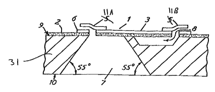
F~g~e 1 ~ihc~ws a ~low 8 nsor in ~ccordance with the pre~elat
illve;ltioA ~O~lp~8~ ;il be~ 1 fabricated from a thin ~nsul~ti~s~
35 fil3~ typ~cally 0.5 m;cro~e~res thicX, th~s fil~ 2 ~ ~o~ted brith
- :
2~
: 3:
metal 3 whlt:h ~8 t~,plc~ 3 ~ r~re~ t~c~ e~l 3
en~ure~ t~a~ the beam 1 18 bot~ ld ~d ~lh~. ~ha ~
p~otet~ 1~ this e~mple, ~out lt~ m~d-polnt ~ uppo~ts 4
constr~lcted ~rom, ~d i~te~ral ~:ft~9 the 6~me ~ulat~ ~ler ~8
5 the besm. The be~m 18 able to pi~ot ~bout the ~xla ~L-X, ~d t~
pi~roe support~ 4 are thin, t~ cally O.S micrometre~ a8 not to
Af ect the ~en~ ty o~ the deYlce at lo~d flow rate~- ~he bea~
~upportet a~otre a s~cu~ductor ~ub~;trate 31,
Ele~tri~al co~ta~t8 llA, llB ~re ~onmed on t~e free e~da o~
~he bea~, ~he e a~t ~ o~e eleotrode of a capaC~tO~- The Ot~er
capac;t~r electrodeæ ~ are fabrlcated directly belo~ the~e.
~ elo~ one h~lf o t~e beam a ~ha~nel 7 i6 formed which
extend~ ~hro~gh ~he ~emiconductor suhstrate 31 ~rom t~e fir8t
major ~urface of the ~bst~ate 9 on w~ch the beam 1 18
fabricated~ to the oppo61te ~ajor sYrface 10 of t~e sub~tr~te.
Thu~ the fluld who e flow i8 being ~ea8ured i~ ~ble to pa~ ri~t
the ~a~ through the 6ub~tr~te 31. A ca~lty 8 i8 for~ed below ~he
other half of the beam 1. Thl~ oavity ~te~d~ only part ~ y
through the su~strate 31 and doe~ ~ot allo~ the p~ssn~e of ~lula
through i~. Thi~ th~n ~llows ~he devlce to oper~t~ ou a '~ull"
principle. Ihi~ mean~ t~at ~he~ the d~vlce i8 put l~ the path o~
a flowing ~luid, bec~u8e onl~ one "th~o~gh" cha~el e~i~t~, there
will be a di~fe~e~ial force ~cro~ the beam and o~l~ the side of
the be¢m ~bo~e thi~ "~hroug~" ch~n~el will e~pe~euce th~8 force.
In ope~tion, a component of fluid flow normal to the majo~
fiu~f~ces of tbe beam 1 i~ either directio~ will cau~e the bea~ 1
to t~i~t ~bout its pi~ot poi~t, wi~h the half o~ tbe bea~ ~bo~
the "throu~h" chan~el ~ov~ng i~ the direct~on of the co0~onent of
fluid flow act;ng upon it.
An ~lectrostatic fo~e is applied to the deYice co~tact~ lLA~
llB in ~uc~ ~ wa~ a~ to ret~rn th~ be~m to it~ equilibrium
position. Thi~ eyuilibrium po~ition is deflned ~s beln~ ~hen the
~ontact gap ~t zero ~luid flow (Yo ;~ Figure 2) 18 eq~al o~l both
~Ides vf the be~, i.e. betwee~ nd 6 and llB and 8.
The amowlt of electro tatic forc~ req,uired and t~ oont~ct~
: ~:
to ~hloh lt ~8 applle~il 18 de~e~éd b~ comp~ ~ ~
be~ee~ the co~t~cts 11~, 6 o~ ~e ~d ~ th~ ~e~ to th~ ~ th~ .
other e~d o~ the be~m llB, 8. ~ tl~B ~t~y ~ e~ ln d~l tr~c
const~t o~ the fl~id do not af~c~ the mea~ t o~ 1uid
S flow. The ~.~pper l~ c o~ the r~e o~ fluld ~ ra~e~ o~re~ wh-~ch
the de~ç is capable of worlclng i8 limlted onl~ b~ ~he a~olmt of
volta~e available to apply suf~oieut elect~o~atic ~orce.
I~ th~ way the fluid ~relocity ma~ be obtal~ed b~ ut~liz~n~
the equ~tion o~ motio~ ~f th~ oYerall ~ygte~ as~d st~dard feedbacl~
10 control t~eo~;~r. In pr~ot;c~, th~ de~l~ction o~ th~ beam iB ~mall
a~ the resto~In~ for~e o.f t~e h~ge i~ ~mall compared to th~
fo~ce due to the ~luid flcw.
Referring now also to Fig~Lres 2 a~d 3
V = ~ r ~br~Q2 volt~
4 A
where~ Re~ulting Elect~static srce br~in~ ~e
beam back to e~u~lib~ium.
- I~eDsity oP 1uid ~1~g/~3)
v = ~elocity o~ flu~d ~ml~
b = ~idth of bea~ (m)
r = length of be~ to h~~ OD one s~de~ (3)
~o = cont~ct g~p at zero flu~d flow (m~
- pe~nitt~Yity 0~ ee ~pace
A - A~ea of ove~lap o~ top ~d bo~to~ cont~cts.
A functio~l block diagram of one suitable ~rcuat for
25 operatiu~ 6uch a deYice 16 sho~n i~ Fi~. 3.
A si~le wa~e volti~ge VO i8 applied acros8 the c~tacts 11
a~d llB. Amp1i~e~g l~A and 12B con~/e~t th~ c~pacitancec
betwee~ the6e con~act~ ;~to a volt~ge ~ven by:-
Y~ = o _, ~ V~ V ~
L~ C~ capacl~anc~ ~etwee~ cne ~lectrlc~lcorltact~ o~ ~he beam llA~ llB L~d the e;Lectrode~ 6 re~pect~vely.
CF ~8 the feedback caE1acitan~e aro~d the ~npl~lerlt 1
a21d l~iS.
After a~pli~icat~on by ~mpli~er~ 13A and 138 ~nd
35 rectificatio~ ~y 14A~ d 143 ~he ~roltage~ aLre comp~ d i~ a
:
2i~
dlfference ~pllf~er tS. The ~ of ~3~ J ad3~te ~o tb4
~i.th ~ero fluld veloc~ty th~ ou~put ~ro~ thc diiE~r~
ampllfler 1~ zero.
The output fro~3 the difference ~snplier 1~ of po~t~e o~
5 ne~ati~e al~ depe~dlng ~pOIl whe~he:s capRC~t~Ce Cl or C2 1 the
~eate~. ~he swltch 17 ~ de~l~ne~ to apply t~e ~p~f~ed ~rror
~ol~e f~cm 16 ~o ~he CozltactB wi~b, tl~e ~lle~t cap~cit~ce~
the re~lllt~ng electro~;t;~tic ~ors~ b~g~ng ~he beYln baclc ~o lt~
e~uilibr~um posltlo~.
The ~q~are root ~unction perfo~ed b~ l~A and 18B ~
impor~t addition ~c~ th~ ~ ci~:c~l t afi ~,t e~su~es the eq~ o~ of
motio~ for the ovF~rall sy tem (includ~:ng the 10w ~e~sor~ ig ;h
ttle for~ of a linear di~e~en~lal equatic~ ~d ~ e ~ readll~
~naly~ed u~in~ gt~dard feedbacl~ cor~trol theo~
Figurc~ 4~ to 4rl lllust~ate a preferred met~od of
f~bricatio~ of the de~ce, the met~od ~fi de~cribed a~ foll~ws:-
a) ~ monocrys~lline EiliCOl~ W~ 2' 20 ~:~picall~ 350
micro~eters. ~hick is prep~r~d with the n~;o~ ~u~nccs 1
the 100 plane.
20 h) A laye~ 21 of all electric~ ula~g m~ter~
sil~on dioxide~ qIl$con ox~itri~{~ o~ s~ .c~ D~ de,
typicall~r 0.5 microme~re6 thiCk i deposited on ~e upper a~d
lo~er surfa~e~, (Figure 4~)
c) At thi~ and subseq~ent 8~s~e8, s~oclate~ electr~a~
2S circuits m~y ~e def~ned i~ the ~e~,
d~ La~er 21 i~ ~lectively etched to defi~e the be~ and it~
piYots 4. ~Fig~re 4B3
e) la~er~ of 6uit~ble ~etal~ ~uch as chromlu~ tgpicall~ 0~1
micrometer thi~k followed by gold ty~icall~ 0.3 ~cromete~
thic~, are depo~;ted o~ ~he top i~s-llat~ng layer and pattenned
photolithog~aphic~lly to defi~e f~xed electrodes 6 and bea~
plating 3 (Fi~ure 4C~.
) Photo~e~ist i6 ~p~n outo the lower i~sul~tor a~ the
in~ulator 1~ p~tte~ned and eeched to ~efi~e ths open oha~el 7
~Fig~re 4~).
2~
: 6:
rer of photoresl0t t~ 3 D~cr~ater~ G~
depo~Jted to d~ t~e gap ~et~en th~ up~r ~
COl~t~l!tB, and ~8 patter~e~ to de~ne ~b,e b~ pla'c~ ~Lrea 3.
h) A pl~tlng bg~ 23~ tgp~ally O.~ mlcrometers t~ nd of
5 an~r sultable me~al ~uch ~8 gold, ~Q depo8~ted OV~I~ the ~ole
upper surface.
i~ Photo~e~lst 24 t~pic~ll;sr 4 to 5 m~s:ro~eters t~l~GtC ~
depocited o~er the top s~rface a~d ~?attea~ed to deflLe edges of
the top co~ct~ llA a~ 11~3.
j~ Expo~ed met~l is pl~ted with . sui.t~71e met~l ~uc~ a~ gold
2S to ~ tb~ckne~ o~ tgpî~ally 3 ~cro~eter~ ~hlch ~tren~hen3
the bea~ to re~o~e s~e~s efect~ an~ al60 pro~ide~ the top
contacts llA a~d llB.
~) resist 24, exposed ~lating ba~e 23, and re~i~ 22 are all
lS removed.
1) me channel 7 and the cav~t~ ~ are f~rmed ~ further
anisotropic etchin~.
The inven~ion ~8 ~ot ll~ed b~ the lll~trated
embod~men~; ot~er ~t~uctu~e~ a~d w~thod~ of sanu~actu~e
thereof, toget~er w~th sultable c~rcu~t~ wlth~ the ~n~e~tiYe
principleg ~ill ~e appa~e~ tu tho~e with ~klll~ 1~ t~e art.
' ' ' .