Note : Les descriptions sont présentées dans la langue officielle dans laquelle elles ont été soumises.
2 0 1 8 8 0 8
POWER SEMICONDUC~OR PACKAGE
1. Technic~LEi~
This in~ention relates to semiconductor devices
and, more particularly, to power semiconductor device
packaging.
2. Discussion
Prior art power semiconductor pacXages include the
standard TO-228 and TO-254 semiconductor packages.
Both of these packages are similarly hermetically
sealed. However, when these packages are mounted
perpendicular to the main- heatsink, they require a
daughter or intermediate heatsink to thermally connect
the chip to a main heatsink. The daughter heatsink
contributes to poor heat transfer because it consists
of another metal to metal thermal contact between the
semiconductor chip and the main heatsink. The need for
a daughter heatsinX also increases the spacing required
for installing these power semiconductor devices.
Finally, replacement of present semiconductor packages
is inconvenienced since the daughter heatsink must also
be removed.
~P
... .
, , .. , . ~ , . ~ .,
-` 2018808
la
SUMMARY OF THE INVENTION
Various aspects of the invention are as follows:
A power semiconductor device package, said
package comprising:
a semiconductor chip encapsulated in a body
with two opposite major surfaces and two opposite end
surfaces, a plurality of pins connected to the chip and
extending ~rom one end surface of the body;
a relatively thick thermally conductive back
having two oppo~ite ma~or ~ur~ace~ and two oppo~ite end
sur~ace~, 5aid body being mounted to one ma~or ~ur~ace
o~ the back so that an end surface of the body is
substantially flush with an end surface of the back:
and
each end surface of the bacX having at least
one mounting hole therein for receiving external
fasteners whereby the pin~ can be connected to a
printed wiring board which is mounted ad~acent one end
surface of the back and wherein a heatsink can be
directly connected to an opposite end surface of the
back thereby eliminating the need for intermediate
heatsink~ and simplifying the replacement of the power
semiconductor device package.
A power o-miconductor devico mounting
arrangement co~prising:
a printed wiring board having a plurality of
openings therein for receiving pins of a power
semiconductor device package;
a heatsink having a plurality of mounting
openings therein;
lb 2 01 8808
a power semiconductor device package having a
body with two opposing major surfaces and two opposite
end surfaces with pins extending from one end surface;
said semiconductor device package further including a
relatively thick metal back having a pair of opposing
major surfaces and a pair of end surfaces, one major
sur~ace of the semiconductor body being mounted to a
ma~or sur~ace o~ the back 50 that an end surface o~ the
body i~ substantially ~lush with an end surface o~ the
back, èach end Bur~ace of the back having mounting
holes therein:
- first fasteners extending through the
openings in the printed wiring board into the mounting
holes in one end surface of the back, said pins
extending through the pin receiving openings in the
printed wiring board for making electrical connection
thereto, and second fasteners extending through the
mounting openings in the heatsink into the mounting
holes in the opposite end sur~ace o~ the back; and
whereby the back is in direct contact with
the heatsink thereby eliminating intermediate heatsinks
~or cooling and wherein the arrangement ls compact and
permits easy repla¢ement Or th~ ~emiconductor package
ii necessary.
By way of added explanation, in accordance with an
aspect of this invention, a power semiconductor device
package is provided which includes a main body having
two opposite
, .,
2018808
--2--
major surfaces and two opposite end surfaces. The body
encapsulates power semiconductor chips in its interior.
In addition there is a plurality of pins projecting
from one of the end surfaces which are connected to the
semiconductor chip. One of the major surfaces is
mounted to a relatively thick metal back. This back
consists of two opposite major surfaces as well as two
broad, oppo~ite end surfaces. Both the end surfaces o~
the ~ack contain a plurality of holes to accommodate
fastening devlce5.
A mounting arrangement for this package includes a
printed wiring board with a plurality of openings
therein for receiving pins of the semiconductor package
as well as mounting screws for the package. The pins
of the package are installed through the openings in
the printed wiring board and soldered in place in order
to create electrical contact. one end surface of the
back is fastened to the printed wiring board through
the appropriate mounting openings in the board and
holes in the back of the package. The other end
surface of the package body is fastened to a heatsink
also having a plurality of mounting openings.
This invention provldes hermetically eealed power
semiconductor packages which minimize spacing while
maximizing thermal efficiency. The invention
eliminates the need for a daughter heatsink which was
previously required in similar semiconductor packages,
thus simplifying replacement and providing an efficient
means of channeling excess heat generated by most power
semiconductor chips.
_
BRIEE DESCRIPTION OF THE DRAWINGS
The various advantages of the present invention
will become apparent to those skilled in the art after
Zt)18808
--3--
reading the following specification and by reference to
the drawings in which:
FIG. 1 is a side view of a semiconductor package
made in accordance with the teachings of the present
invention;
FIG. 2 is a front view of the package shown in
FIG. 1;
FIG. 3 is a cros~-sectional view of a typical
mounting arrangement ~or the pacXage in FIG. 1; and
FIG. 4 6hows a front view of the mounting
arrangement shown in FIG. 3.
DETAILED DESCRlPTlOn OF T~B PR~FERRED EMBODIMENT
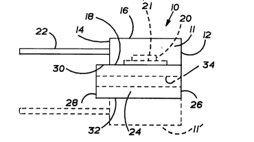
Referring now to FIGS. 1 and 2, the semiconductor
device package 10 includes a semiconductor chip 20
which is mounted on a ~ubstrate 21 which, in turn, is
surrounded by an encapsulating body 11 made of copper,
Xovar, molybdenum, beryllia or alumlna. The body 11
has two oppo~ite major surfaces 16 and 18 and two end
surfaces 12 and 14. A number of pins 22 connected to
the semiconductor chip 20 ~e.g. by conventional wire
bonds) extend out from the encapsulating body. The
en¢apsulating body may aontain multlple ~emiconductor
devices if desired. The substrate 21 is bonded in such
a manner to create good thermal contact with a
relatively thick metal back 24. The back 24 is
generally thicker than body 11, as well as being longer
along the axis of the pins 22. By way of- a typical
example, the back 24 is 0.25 inch thick x 0.70 inch
wide x 0.635 long and can be made of a variety of
thermally conductive materials such as aluminum, copper
and the like. The back 24 also has two opposite major
surfaces 30 and 32 as well as two end surfaces 26 and
28. These end surfaces are larqe enough so that
several tapped holes 34 may be drilled from end surface
2018808
26 to end surface 30. These holes 34 accommodate
various fasteners, such as mounting screws which are
used to attach the device 10 to various printed wiring
boards and also to external heatsinks as will be
discussed later herein. A second device ll' may be
added as seen in FIG. 1 to create a "piggy back"
arrangement. The second device is mounted on the other
oppoeite ma~or surface 32 of the bacX 24.
A preferred mounting arrangement for deviae 10 is
shown ln FIGS. 3 and 4. A printed wiring board 38 has
holes 39 drilled therein for fasteners 40 as well as
pin receiving openings 41. The pins 22 of device 10
are inserted through the holes 41 and are soldered into
place through the use of solder joints 42. The metal
back 24 is attached to the printed wiring board 38
through the use of one or more fasteners 40 which
engage the threads in openings 34 to draw the underside
of the board 38 against end surface 28 of the back 24.
The other end surface 26 of the back 24 is similarly
attached directly to an external metal heatsink 44.
The heatsink 44 has several holes 46 drilled into it in
order to accommodate a pair of fa~teners 47.
In view of the foregoing, several advantages may
be appreciated over the prior art. This invention
provides a printed wiring board to heatsinX mounting
structure without the requirement of a daughter
heatsinX. This minimizes spacing in addition to
eliminating the daughter heatsinX for this type of
application. This arrangement provides a very secure
mounting thereby minimizing the detrimental effects of
thermal stresses on the solder ~oints and hermetic,
lead, ceramic or glass seals which may be used. In
addition, it provides a secure mounting of the heatsink
to the package. This also provides a direct metal to
metal contact with high compression for good heat
~0188~)8
transfer. Since the daughter heatsink is not required
in this mounting, it eliminates one metal to metal
thermal contact which would otherwise contribute to
loss of thermal efficiency. The elimination of the
additional daughter heatsink also maximizes ease of
disassembly or reassembly for replacement of defective
semiconductor packages as compared to present
alternatives of 3emicondu¢tor packages. Various other
advantages will become apparent to tho~e skilled in the
art.
_