Sélection de la langue

Search

Sommaire du brevet 2024784 

Énoncé de désistement de responsabilité concernant l'information provenant de tiers

Une partie des informations de ce site Web a été fournie par des sources externes. Le gouvernement du Canada n'assume aucune responsabilité concernant la précision, l'actualité ou la fiabilité des informations fournies par les sources externes. Les utilisateurs qui désirent employer cette information devraient consulter directement la source des informations. Le contenu fourni par les sources externes n'est pas assujetti aux exigences sur les langues officielles, la protection des renseignements personnels et l'accessibilité.

Disponibilité de l'Abrégé et des Revendications

L'apparition de différences dans le texte et l'image des Revendications et de l'Abrégé dépend du moment auquel le document est publié. Les textes des Revendications et de l'Abrégé sont affichés :

  • lorsque la demande peut être examinée par le public;
  • lorsque le brevet est émis (délivrance).
(12) Brevet: (11) CA 2024784
(54) Titre français: SUBSTRAT MULTICOUCHE EMPILABLE POUR LE MONTAGE DES CIRCUITS INTEGRES
(54) Titre anglais: STACKABLE MULTILAYER SUBSTRATE FOR MOUNTING INTEGRATED CIRCUITS
Statut: Réputé périmé
Données bibliographiques
(52) Classification canadienne des brevets (CCB):
  • 356/143
(51) Classification internationale des brevets (CIB):
  • H01L 23/32 (2006.01)
  • H01L 23/00 (2006.01)
  • H01L 23/13 (2006.01)
  • H01L 23/538 (2006.01)
  • H01L 25/065 (2006.01)
  • H05K 1/03 (2006.01)
(72) Inventeurs :
  • WARREN, KEITH O. (Etats-Unis d'Amérique)
(73) Titulaires :
  • LITTON SYSTEMS, INC. (Etats-Unis d'Amérique)
(71) Demandeurs :
(74) Agent: SWABEY OGILVY RENAULT
(74) Co-agent:
(45) Délivré: 1994-01-04
(22) Date de dépôt: 1990-09-06
(41) Mise à la disponibilité du public: 1991-03-15
Requête d'examen: 1990-12-27
Licence disponible: S.O.
(25) Langue des documents déposés: Anglais

Traité de coopération en matière de brevets (PCT): Non

(30) Données de priorité de la demande:
Numéro de la demande Pays / territoire Date
407,045 Etats-Unis d'Amérique 1989-09-14

Abrégés

Abrégé anglais


11

A STACKABLE MULTILAYER SUBSTRATE
FOR MOUNTING INTEGRATED CIRCUITS

ABSTRACT OF THE DISCLOSURE
A substrate is formed from a core substrate of
flexible, low-temperature co-fireable ceramic tape and an
outer substrate of ceramic tape having apertures for
receiving integrated circuits (ICs) therein. The
substrate is heated to form a rigid body which then mounts
the ICs. The rigid body and ICs are covered or at least
partially covered with an insulating glass and heated to
a temperature that fuses the glass but does not harm the
ICs. The resulting structure hermetically seals the ICs
in a single substrate that is insensitive to acceleration
forces.

Revendications

Note : Les revendications sont présentées dans la langue officielle dans laquelle elles ont été soumises.


The embodiments of the invention in which an
exclusive property or privilege is claimed are
defined as follows:
1. A substrate for mounting integrated circuits
having a first substrate with a plurality of
insulated layers and a second substrate with a
plurality of insulated layers, said second
substrate having apertures therein for receiving
said integrated circuits, each of said first and
second substrates being former into a single,
rigid multilayer board having the integrated
circuits mounted within the apertures; wherein
the improvement is characterized by:
a layer of insulating material placed at
least partially over said integrated circuits and
at least partially filling said apertures that
receive said integrated circuits;
said layer of insulating material formed
into a rigid surface over said integrated
circuits on said multilayer board to mount said
circuits rigidly upon said board to be
insensitive to acceleration forces;
said layer of insulating material covering
said rigid multilayer board;
a plurality of said rigid multilayer boards
stacked together into a multistack of rigid
boards; and
said layers of insulating material covering
said rigid multilayer boards bonding said
plurality of boards into one multistack as said
layers form said rigid surface over said
integrated circuits to mount said circuits in
said multistack configuration.
2. The substrate claimed in Claim 1,
wherein:
said layer of insulating material is placed
over said integrated circuits to fully cover said
circuits and to fill said apertures.


3. The substrate claimed in Claim 1, additionally
comprising:
said layers of insulating material having a
plurality of isolated areas therein formed from conductive
material for electrically joining said rigid multilayer
boards within said multistack to each other.

4. The substrate claimed in Claim 1 wherein:
said first and second substrates are formed from
a plurality of layers of low-temperature co-fireable
ceramic tape that is flexible until subjected to heat.

5. The substrate claimed in Claim 1, wherein:
said layer of insulating material is a layer of
non-conductive glass that hermetically seals said
integrated circuits.

6. The substrate claimed in Claim 3, wherein:
said isolated areas of conductive material are
formed from said non-conductive glass made conductive by
the addition to said areas of conductive material.

7. The substrate claimed in Claim 1, wherein:
said first and second layers are formed into a
single rigid multilayer board by heating to a first
temperature; and
said layers of insulating material are formed
with rigid surfaces by heating to a second temperature
approximately one-half that of said first temperature.

8. The substrate claimed in Claim 1, wherein:
said first temperature is about 850°C plus or
minus about 50°C; and
said second temperature is about 380°C to 480°C.

9. The substrate claimed in Claim 1, wherein:


said second substrate is placed on both sides of
said first substrate.

10. The substrate claimed in Claim 1, wherein:
said first and second substrates have conductive
paths thereon and conductive vias therein.

11. A method of manufacturing a substrate for
mounting integrated circuits in a multistack configuration
comprising the steps of:
forming a first core substrate from a plurality
of insulated layers that are flexible until heated;
forming a second outer substrate against said
first substrate from a plurality of insulated layers that
are flexible until heated having a plurality of apertures
therein which are aligned to form integrated circuit
receiving apertures;
heating said first and second substrates into a
single, rigid substrate;
placing integrated circuits into said apertures
in said second outer substrate;
placing a layer of heat setting insulated
material at least partially over said integrated circuits
in said apertures;
heating said insulating material and said
single, rigid substrate and integrated circuits to mount
said integrated circuits rigidly upon said rigid
substrate;
placing said layer of heat setting insulating
material over the full surface of said rigid substrate;
placing two or more rigid substrates into a
stack; and
heating said insulating material and said two or
more rigid substrates and integrated circuits to a
temperature hot enough to melt said heat setting
insulating material but not hot enough to melt said two or


more substrates or to harm said integrated
circuits to mount said circuits in said
multistack configuration.

12. The method of Claim 11, wherein:
said step of heating said first and second
substrates is carried out at about 850°C plus or
minus about 50°C; and
said step of heating said insulating
material is carried out at about 380°C to 480°C.

13. The method of Claim 11, wherein:
said step of forming a second outer
substrate against said first substrate forms said
second outer substrate on both sides of said
first substrate.

14. The method of Claim 11, wherein:
said step of placing a layer of heat setting
insulating material over said integrated circuit
includes covering said integrated circuits and
filling said apertures.

15. A substrate for mounting integrated
circuits having a first substrate with a
plurality of insulated layers and a second
substrate with a plurality of insulated layers,
said second substrate having apertures therein
for receiving said integrated circuits, each of
said first and second substrates being formed
into a single, rigid multilayer board having the
integrated circuits mounted within the apertures;
wherein the improvement is characterized by:
a layer of insulating material placed at


11
least partially over said integrated circuits and
at least partially filling said apertures that
receive said integrated circuits;
said layer of insulating material formed
into a rigid surface over said integrated
circuits on said multilayer board to mount said
circuits rigidly upon said board to be
insensitive to acceleration forces;
said layer of insulating material covering
said rigid multilayer board;
a plurality of said rigid multilayer boards
stacked together into a multistack of rigid
boards;
said layers of insulating material covering
said rigid multilayer boards bonding said
plurality of boards into one multistack as said
layers form said rigid surface over said
integrated circuits to mount said circuits in
said multistack configuration;
said first and second substrates being
formed from a plurality of layers of low-
temperature co-fireable ceramic tape that is
flexible until subjected to heat; and
said layer of insulating material being a
layer of non-conductive glass that hermetically
seals said integrated circuits.

16. The substrate for mounting integrated
circuits of Claim 1, wherein:
patterns of conductive glass paste
surrounded by an insulating glass provide
electrical contact between at least two of said
rigid multilayer boards stacked together into a
multistack of rigid boards.

12
17. The substrate for mounting integrated
circuits of Claim 15, wherein:
patterns of conductive glass paste
surrounded by an insulating glass provide
electrical contact between at least two of said
rigid multilayer boards stacked together into a
multistack of rigid boards.

Description

Note : Les descriptions sont présentées dans la langue officielle dans laquelle elles ont été soumises.


202~784
,' !
:,
.,
,
, Field of the Invention
The present invention relates to a- stackable
multilayer substrate and, more particularly, to a
substrate that mounts integrated circuits (ICs) thereon so
that the integrated circuits are impervious to high
acceleration forces and atmospheric conditions.
~, . .
~;~ Descri~tion of the Prior Art
It is well-known in the prior art to utilize a thin-
film structure that can be formed from multilayers of low-
temperature co-fireable ceramic tape with power and ground
connections between the multilayers. The so-called co-
fireable ceramic tape is a flexible substrate before
heating manufactured by various companies including DuPont
who sells its product under the trademark Green Tape. The
thin and flexible material becomes rigid after it is
subjected to heat as by firing in an oven. DuPont and
other companies market this material for high-density
packages of ICs with conductive layers sputtered onto the
multilayers of the ceramic tape before its firing.


.,., ~
.. ...
: .~ . . . .

-` 2~2~7~4


SUMMARY OF THE IN~ENTION
It is an object of the present invention to utilize
the known capabilities of the low-temperature co-fireable
ceramic tape to form a substrate for mounting integrated
circuits that will enable the circuits to withstand high
acceleration forces and severe atmospheric conditions
applied thereto.
It is another object of the present invention to
eliminate the need for mechanical metal packaging usually
associated with integrated circuits.
In accomplishing these and other objects there is
provided a first substrate formed from multilayers of low-
temperature co-fireable ceramic tape which acts as a core
upon which the integrated circuits (ICs) may be mounted.
Conductive paths and pads may be sputtered or screen
j printed upon the multilayers and conductive vias may be
,~ mounted in through holes therein to carry electrical
signals from one layer to the other. On one or both sides
of the core are outer layers of ceramic tape which may be
provided with apertures therein for receiving the
integrated circuits. The outer layers may also be screen
printed to form conductive paths and pads for the ICs
mounted within the apertures therein. After the core
layer and its component receiving, outer layer or layers
are formed, the resulting substrate is fired to create a
rigid multilayer circuit board.
Thereafter, the rigid multilayer circuit board may be
; assembled by mounting appropriate ICs into the apertures
formed within the outer layers of the multilayer board.
Each individual rigid multilayer printed circuit board is
then coated with a non-conductive sealing glass frit to
cover or at least partially cover the ICs~ Several rigid
multilayer circuit boards may then be joined together in
a stack with the ICs mounted therebetween. The stack of
multilayer boards may be joined by heating the non-
conductive glass coated upon their surfaces. The ICs may


i

2 ~ 8 ~

,, .

be electrically connected between the stacked boards by
forming isolated areas of the non-conductive glass into
conductive frits. Thereafter, the stacked, sandwiched
assembly is fired at a temperature high enough to fuse the
glass but low enough so as not to damage the ICs. The
resulting package is a rigid package with firmly mounted
- ICs encased in the fired non-conductive glass to form an
electronic package that is unaffected by high acceleration
forces and is hermetically sealed.
' 10
DESCRIPTION OF THE DRAWINGS
- A better understanding of the invention will be had
after consideration of the following specification and
drawings, wherein:
15FIG. 1 is a cross-sectional view showing a typical
single co-fired substrate of the present invention; and
FIG. 2 is a perspective view showing several single
co-fired substrates in a preassembly configuration before
stacking.
DESCRI~TION OF THE PREFERRED EMBODIMENT
Referring now to the drawings, FIG. 1 shows a cross-
sectional view of a typical multilayer substrate 10 having
a core 11 formed from three, five, or more layers of low-
temperature co-fireable ceramic tape substrate 12 that are
flexible before firing. Such tape is manufactured by
DuPont Electronics under the trademark Green Tape. on one
or both sides or in between the multilayers of ceramic
tape 12 are various patterns of electrically conductive
paths 13 which may be deposited by known techniques, such
as screen printing or vacuum sputtering. Joining the
various layers of ceramic tape 12 are a plurality of vias
,14 formed by small plugs of conductive material, such as
gold or conductive glass, which may be screen printed into
through holes formed in the layers of tape 12. On one or
both sides of the core 11 of the multilayers of tape 12


i~

,....... . . ~ . -
.:. : ~ .- , ;.

: . ,.

4 202~78~

are second substrates formed by outer multilayers of
ceramic tape I5 and 16 provided with apertures 18 therein,
as by a punch process. The multilayers that form
substrates 15 and 16 are stacked to form apertures 18
~herein with step-like shoulders 19 for mounting suitable
ICs 20. It will be seen in FIG. 1 that the ICs 20 have
electrically conductive leads 22 which are aligned with
the steps 19 of apertures 18. Suitable conductive paths
and pads, not shown, may also be mounted on steps 19 to
receive the leads 22.
After the multiple layers 11, 15 and 16 of the co-
fireable ceramic tape are formed but before the ICs are
inserted, the assembly may be fired in an air atmosphere
in an oven at about 850C plus or minus about 50C for
forming all layers into a rigid multilayer circuit board.
While layers 11, 15 and 16 are shown in a plane, it will
be understood that they may also be shaped into non-planar
configurations. After the layers 11, 15 and 16 are formed
into the rigid board, the ICs 20 are inserted into
, 20 apertures 18 and their leads 22 attached to appropriate
conductive paths or pads 13 or vias 14 on the steps 19 of
apertures 18, as by soldering or spot welding. Before and
after the assembly of the ICs 20, the rigid multilayer
circuit board may be cleaned in an 2 atmosphere, for
example.
Thereafter, the rigid substrate 10 may be coated by
screen printing with a suitable non-conductive sealing
glass frit 24 which covers or at least partially covers
the ICs 20 and fills or partially fills the apertures 18,
only one of which is shown in FIG. 1. The sealing glass
frit may be one of several kinds including, but not
limited to, sealing glass manufactured by Corning Glass
Works as its sealing glass, Corning Codes 7585 or 7589.
The ICs need only be partially covered when concerned with
high acceleration forces upon the IC leads 22. Here, the
sealing glass frit need only cover the leads 22. In other
* Reg. ~.M.

.,

,. -: . ~ , . : .

: : . . ,~, . : ,,

2a2~784

applications, it may be necessary to fully cover the
structure of ~he ICs.
The glass frit which covers or partially covers the
IC leads can be formed from several layers of glass or
s formed from a single layer. Further, the glass can be
selected to have a density and coefficient of thermal
expansion close to that of the silicon material of the
ICs. The non-conductive glass frit may be made conductive
in certain isolated areas by silver loading the non-
conductive glass with, for example, Amicon CG-932-4D
silver/glass conductive adhesive, as shown in FIG. 1 at
25. In this way, certain areas of the surface of the
single substrate 10 may be made conductive by the presence
of the conductive glass frits 25 to electrically join one
single substrate to another, as discussed below.
FIG. 1 shows, by way of example, a wiring circuit
formed by a via 14 which passes through the layers 12 of
core substrate 11 from a pad 13 to a conductive path 13'
and then to a second via 14'. The conductive path 13'
could connect to a lead, not shown, on the IC 20 shown on
the lower, left-hand surface of core 11. The conductor
13' also connects through the second via 14' to a second
conductive path 13'' to a third via 14'' and then to the
lead 22 of the IC 20 on the upper, left-hand surface of
core 11. In the example shown, a conductive glass frit 25
flows into apertures 26 in the outer layers 15 to
electrically connect the outer surface of the substrate 10
to the wiring circuit just described. It will be
understood that the non-conductive glass frit 2~ may be
flowed or screen printed over the full outer surface of
substrate 10 using, for example, 80 mesh stainless steel
screen and 100 mesh frit.
To complete the assembly of the single substrate 10
of FIG. 1, the substrate and its non-conductive and
conductive frits 24 and 25, respectively, are placed in a
conventional oven in an air atmosphere and heated to about
* Reg. T.M.


`' , ' ,. ' "; . `' '. ' .''' ' ' " .'' "' : ~' ' ' . .
' . ' . ~: ' ' ' ' , ., ': ,'.' . ;.' ' ' . '. ; ' ' ' '

6 2~2478~

380OC for the Corning 7585 sealing glass or to about 4800C
for the cornlng*7589 sealing glass. These temperatures
are hot enough to melt the glass and yet low enough so as
not to harm the ICs 20.
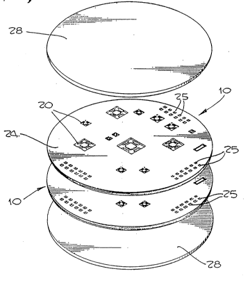
As shown in FIG. 2, a plurality of individual
substrates 10 may be stacked upon each other to form a
sandwiched construction. The stack is arranged with non-
conductive sealing glass 24 covering the outer surfaces of
s substrates 10 and conductive glass frits 25 at appropriate
isolated areas in the surfaces of the substrates in
contact one with the other.
Thereafter, the sandwiched assembly may be fired
` again at a temperature high enough to melt the glass but
~ low enough to prevent damage to the ICs 20. In the
'~ 15 preferred embodiment, the temperature is about 380C for
Corning* 7585 sealing glass and 480C for Corning* 7589
sealing glass. The non-conductive glass 24 thus seals the
package into a rigid structure, while the conductive glass
25 creates electrical contacts between the individual
` 20 substrate 10.
The resulting structure of multistacked substrates 10
, is rigid and highly resistant to accelerational forces.
Further, the resulting structure hermetically seals the
` ICs 20 and eliminates the need for machined metal packages
normally associated with the ICs 20.
As seen in FIG. 2, the assembly may be completed
through the use of appropriate covers 28 which may be
joined to the sandwiched stack of substrates 10 using the
same non-conductive glass 24 used to seal the ICs in their
apertures 18.
* Reg. ToM~
.:


~;
,,.~


,;~ :. .: . :: ,.: ;~ - .. .. :

Dessin représentatif
Une figure unique qui représente un dessin illustrant l'invention.
États administratifs

Pour une meilleure compréhension de l'état de la demande ou brevet qui figure sur cette page, la rubrique Mise en garde , et les descriptions de Brevet , États administratifs , Taxes périodiques et Historique des paiements devraient être consultées.

États administratifs

Titre Date
Date de délivrance prévu 1994-01-04
(22) Dépôt 1990-09-06
Requête d'examen 1990-12-27
(41) Mise à la disponibilité du public 1991-03-15
(45) Délivré 1994-01-04
Réputé périmé 2000-09-06

Historique d'abandonnement

Il n'y a pas d'historique d'abandonnement

Historique des paiements

Type de taxes Anniversaire Échéance Montant payé Date payée
Le dépôt d'une demande de brevet 0,00 $ 1990-09-06
Enregistrement de documents 0,00 $ 1991-01-25
Taxe de maintien en état - Demande - nouvelle loi 2 1992-09-07 100,00 $ 1992-08-19
Taxe de maintien en état - Demande - nouvelle loi 3 1993-09-06 100,00 $ 1993-08-13
Taxe de maintien en état - brevet - nouvelle loi 4 1994-09-06 100,00 $ 1994-08-12
Taxe de maintien en état - brevet - nouvelle loi 5 1995-09-06 150,00 $ 1995-08-10
Taxe de maintien en état - brevet - nouvelle loi 6 1996-09-06 150,00 $ 1996-06-26
Taxe de maintien en état - brevet - nouvelle loi 7 1997-09-08 150,00 $ 1997-06-19
Taxe de maintien en état - brevet - nouvelle loi 8 1998-09-08 150,00 $ 1998-06-22
Titulaires au dossier

Les titulaires actuels et antérieures au dossier sont affichés en ordre alphabétique.

Titulaires actuels au dossier
LITTON SYSTEMS, INC.
Titulaires antérieures au dossier
WARREN, KEITH O.
Les propriétaires antérieurs qui ne figurent pas dans la liste des « Propriétaires au dossier » apparaîtront dans d'autres documents au dossier.
Documents

Pour visionner les fichiers sélectionnés, entrer le code reCAPTCHA :


Pour visualiser une image, cliquer sur un lien dans la colonne description du document. Pour télécharger l'image (les images), cliquer l'une ou plusieurs cases à cocher dans la première colonne et ensuite cliquer sur le bouton "Télécharger sélection en format PDF (archive Zip)" ou le bouton "Télécharger sélection (en un fichier PDF fusionné)".

Liste des documents de brevet publiés et non publiés sur la BDBC .

Si vous avez des difficultés à accéder au contenu, veuillez communiquer avec le Centre de services à la clientèle au 1-866-997-1936, ou envoyer un courriel au Centre de service à la clientèle de l'OPIC.


Description du
Document 
Date
(yyyy-mm-dd) 
Nombre de pages   Taille de l'image (Ko) 
Abrégé 1994-07-09 1 26
Page couverture 1994-07-09 1 28
Revendications 1994-07-09 6 223
Dessins 1994-07-09 1 38
Description 1994-07-09 6 300
Dessins représentatifs 1999-07-16 1 18
Correspondance de la poursuite 1990-12-27 2 46
Correspondance reliée au PCT 1993-10-12 1 29
Correspondance de la poursuite 1993-02-19 5 160
Lettre du bureau 1991-03-18 1 18
Demande d'examen 1992-08-21 2 83
Taxes 1996-06-26 1 51
Taxes 1995-08-10 1 62
Taxes 1994-08-12 1 63
Taxes 1992-08-19 1 36
Taxes 1993-08-13 1 41