Note : Les descriptions sont présentées dans la langue officielle dans laquelle elles ont été soumises.
2025800
SPECIFICATION
Title of the ~vention
EI,ECTRODE FOR ELECTRICA~ CONNECTION TO OXIDE
SUPERCONDUCTOR AND METHOD FOR FORMING THE SAME
Background of the Invention
Field of the invention
The present invention relates to a superconductor device using a
superconductor of compound oxide, and more specifically to an electrode
for electric connection to a compound oxide superconductor which can be
effectively implemented in a superconductor device using the compound
oxide superconductor, as well as a method for forming the same
electrode.
Description of related art
In applications of various types of compound oxide superconductors
(called simply "oxide superconductor" hereinafter), superconductor
electronic devices and superconductor wirings for electronic devices are
ones of fields most hopefully expected to be put into practical use.
Josephson devices, SQUIDs, superconductor transistors and
superconductor circuit wirings forrned of oxide superconductors have
been already reported.
In general, superconductor devices include superconductive
conductors or wirings which allow a so-called superconducting current to
flow therethrough. However, in all of superconductor circuits and
devices, the superconductive conductors or wirings have to be electrically
-1- ~
2~Z58~}0
connected to circuits or devices which operate under a normal conduction
condition.
For this purpose, in the above mentioned superconductor devices,
an electrical connection has been realized by using a thin metal wire such
as an Au wire which is called a "bonding wire". If the superconductor is
a metal superconductive material, the bonding w;re can be fixed and
electrically connected directly to a portion of the metal superconductor.
However, if the superconductor is an oxide superconductive material, it is
difficult to fix or secure the bonding wire to a portion of the oxide
superconductor. In the case of the oxide superconductor, therefore, a
metal electrode has been deposited on a portion of the superconductor by
means of vacuum evaporation of noble metal such as Au (gold), and
thereafter, a bonding wire has been fixed and electrically connected to the
metal electrode thus formed on the oxide superconductor. Since the noble
metal typified by Au is very low in reactivity, it will not give an adverse
effect to the oxide superconductor. In addition, even if the noble metal
typified by Au is in contact with air, it is hardly oxidized. In this point,
the noble metal typified by Au is suitable for the elec~rode for the oxide
superconductor.
However, the noble metal typified by Au does not have a good
adhesion or bonding property to the oxide superconductor, and therefore,
a contact resistance has often become large. Therefore, the
superconductor device in which only a very small amount of electric
current is flowed has become unstable in operation, and cannot often exert
an expected performance.
Furthermore, when a metal electrode is formed on a portion of an
oxide superconductor, after a metal film is deposited on an oxide
2025800
superconductor thin film, the metal film is patterned. It has been an
ordinary practice to perform the patterning by using a photolithography.
The following is one example of a "lift-off" process for forming a
metal electrode on a thin film of oxide superconductor.
First, a thin film of o~cide superconductor is formed on a substrate,
which has been properly selected dependently upon the kind of an oxide
superconductor to be formed. For example, the substrate is formed of
MgO. In addition, the thin film of oxide superconductor is deposited by
means of sputtering, MBE (molecular beam epitaxy), CVD (chemical
vapor deposition) or other suitable processes.
Then, a photoresist layer is deposited on the thin film of oxide
superconductor, and patterned so that an opening for allowing deposition
of metal electrode is formed in the deposited photoresist layer. In the
opening of the patterned photoresist layer, the thin film of oxide
superconductor is exposed.
Furthermore, metal is deposited by, for example, vacuum
evaporation, so that the metal is deposited directly on the thin film of
oxide superconductor exposed in the opening of the pattern photoresist
layer.
Thereafter, the photoresist layer is removed, so that the metal layer
deposited on the photoresist layer is removed together. Thus, the metal
layer remains only on a position of the thin film of oxide superconductor
corresponding to the opening of the photoresist layer. Namely, a metal
electrode having a configuration corresponding to the opening of the
photoresist layer is formed on the thin film of oxide superconductor.
However, the above mentioned conventional metal electrode
forming method is disadvantageous in that, since the photoresist layer is
2025800
deposited directly on a surface of the thin film of oxide superconductor,
an interfacial reaction occurs, and therefore, the characteristics of the
oxide superconductor is deteriorated. In addition, in the process of the
photolithography, since the oxide superconductor is in contact with an
~lk~line developing liquid and a cleaning water, the characteristics of the
oxide superconductor is further deteriorated.
SllmmAry of the Invention
Accordingly, it is an object of the present invention to provide a
metal electrode for electric connection to an oxide superconductor, which
has overcome the above mentioned defect of the conventional one and
which has a good adhesion or bonding property to the oxide
superconductor and a sufficiently low contact resistance.
Another object of the present invention is to provide a method for
forming a metal electrode for electric connection to an oxide
superconductor, without deteriorating the characteristics of the oxide
superconductor.
According to the present invention there is provided a metal electrode
formed on an oxide superconductor thin film for electric connection to the
oxide superconductor, the metal electrode including a first layer of Ag
(silver) in direct contact with the oxide superconductor thin film, and a
second layer formed on the first layer, the second layer being formed of noble
metal excluding Ag.
According to another aspect of the present invention, there is
provided a method for forming a metal electrode on an oxide
superconductor layer for electric connection to the oxide superconductor
layer, comprising the steps of forming a first layer of Ag to cover a
X
2025800
whole surface of the oxide superconductor layer, and forming a second
layer of noble metal excluding Ag, to cover a whole surface of the first
layer, thereby to form a double metal layer, and patterning the double
metal layer so as to form a metal electrode composed of the double metal
layer.
As seen from the above, the metal electrode in accordance with the
present invention for electric connection to the oxide superconductor is
mainly characterized in that the metal electrode is composed of two
layers, namely, a first layer of Ag in direct contact with the oxide
superconductor, and a second layer formed on the first layer and formed
of noble metal excluding Ag. Since Ag is remarkably low in reactivity to
oxide superconductors, Ag will never give an adverse influence to the
oxide superconductor. In addition, Ag has a low contact resistance with
oxide superconductors and an excellent adhesion or bonding property to
oxide superconductor. This is a characteristics peculiar or inherent to
Ag. The electrode in accordance with the present invention utilizes this
characteristics of Ag.
On the other hand, Ag is easily oxidized in air. In this aspect, Ag is
not preferable as an electrode material. However, noble metal such as
Au, excluding Ag, is hardly oxidized in air. Therefore, in this aspect, the
noble metal excluding Ag is preferable as an electrode material.
However, the noble metal excluding Ag is poor iIl bonding property to
oxide superconductor, so that a substantial contact resistance often occurs.
Thus, in order to realize a metal electrode which has a good
~onding property to oxide superconductor without adversely affecting the
oxide superconductor, and which is never easily oxidized in air, the metal
electrode in accordance with the present invention is composed of a
2025800
double metal layer having such a construction that a portion in direct
contact with an oxide superconductor is formed of an Ag layer and a
portion in contact with air is folmed of a layer of noble metal excluding
Ag, for example, Au or Pt (platinum).
Preferably, a thickness of the Ag layer and a thickness of the noble
metal layer formed on the Ag layer are in a range of 0.01 ~lm to 1 ~m
and in a range of 0.05 ~m to 1 ~lm, respectively. If the thickness of the
Ag layer is less than 0.01 ,um, the Ag layer has no effect of protecting the
oxide superconductor. On the other hand, even if the thickness of the Ag
layer is greater than 1 ,um, the effect of protecting the oxide
superconductor is not increased, and rather, a long time becomes required
for removal of unnecessary portion of the metal layer after a
photolithography process. Similarly, if the thickness of the noble metal
layer is less than 0.05 ~m, the noble metal layer has no effect of
protecting the Ag layer, and is not sufficient to allow the electrode to
function. On the other hand, even if the thickness o~ the noble met~l layer
is greater than 1 ,um, the effect of protecting the Ag layer is not
increased, and rather, a long time becomes required for removal of
unnecessary portion of the metal layer after a photolithography process.
Therefore, the above mentioned ranges of thickness are preferred.
The method in accordance with the present invention is
characterized by covering a whole surface of an oxide superconductor
layer with a double metal layer composed of a Ag sub-layer and another
sub-layer of noble metal excluding Ag, and then, patterning the double
metal layer into a form of an electrode. In this method in accordance
with the present invention, since the oxide superconductor layer is in
direct contact with neither photoresist nor developing liquid, the
~ 2025800
characteristics of the oxide superconductor will never be deteriorated by
the photoresist or the developing liquid.
I~e metal electrode in accordance with the present invention can be
fabricated by using a deposition process which has been used for
fabrication of conventional electrodes. In this connection, it is preferred
that after formation of the double metal layer, the metal electrode in
accordance with the present invention is heated so as to improve an
adhesion or bonding property between the Ag layer and the oxide
superconductor layer. Preferably, the heat treatment is perfolmed in a
range of 300C to 580C. If the heating temperature is less than
300 C, the heating treatment is not so effective in improving the bonding
property. On the other hand, if the heating temperature is greater than
580 C, a reaction layer is formed, so that the characteristics of the oxide
superconductor is deteriorated. It is more effective if the heating is
performed in atmosphere of oxygen. In this case, the heating processing
is preferably perfo~ned after completion of fonnation of the second layer
of noble metal excluding Ag, in order to protect the Ag layer from
oxidation.
Furthermore, in the method of the present invention, the etching
after photolithography is preferably performed by a dry etching process,
for example, an ion beam etching using inert gas such as Ar, an ECR
(electron cycroton resonance) etching, an RF (radio frequency) plasma
etching, etc. These etching processes are very preferable, since a physical
etching is realized by charged particles without chemical reaction, and
therefore with less influence to the oxide superconductor.
The above and other objects, features and advantages of the present
invention will be apparent from the following description of preferred
2025800
embodiments of the invention with reference to the accompanying
drawings. However, the examples explained hereinafter are only for
illustration of the present invention, and therefore, it should be
understood that the present invention is in no way limited to the following
examples.
Brief Description of d~e Drawings
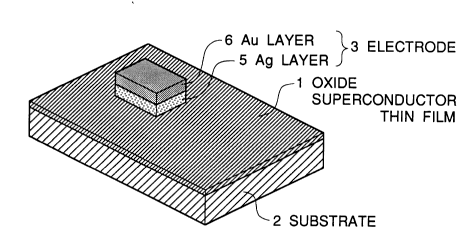
Figure 1 is a diagrammatic perspective view illustrating a structure
of a metal electrode in accordance with the present invention for an
electric connection to an oxide superconductor;
Figures 2A and 2B illustrate a method of measuring a contact
resistance in the metal electrode for the oxide superconductor, and
Figures 3A to 3F illustrate one embodiment of the process in
accordance with the present invention for fabricating the metal electrode
in accordance with the present invention for an electric connection to an
oxide supcrconductor.
Description of the Preferred embodiments
A metal electrode in accordance with the present invention having a
configuration as shown in Figure 1 and a conventional metal electrode
were formed on various types of oxide superconductor layers, and
comparison was performed about characteristics of the electrodes. As
shown in Figure 1, on a thin ~ilm 1 of an oxide superconductor formed on
an insulative substrate 2, there is forrned a metal electrode 3 constituted of
an lower metal sub-layer 5 of Ag and an upper metal sub-layer 6 of Au.
In examples explained hereinafter, a contact resistance in a metal
electrode for electric connection to an oxide superconductor was
- 2025800
measured by using a so-called "three-terminal method" and a so-called
"four-terrninal method" in combination.
First, as illustrated in Figure 2A, conventional electric contacts Cl
and C2 and an electric contact or electrode C3 in accordance with the
present invention are formed on the oxide superconductor thin film 1.
~n electric current I is flowed between the contacts Cl and C3 and is
measured by an ammeter 7. On the other hand, a voltmeter ~ is
connected between the contacts C2 and C3 SO that an electric voltage V
between the contacts C2 and C3 iS measured by the voltmeter 8. Here, it is
assumed that contact resistances at the contacts Cl, C2 and C3 are r" r2
and r3, respectively, and an equivalent resistance in a portion of the
superconductor thin film 1 between the contacts C~ and C3 is R. It is also
assumed that an internal impedance of the voltmeter 8 is infinite.
Under the above mentioned arrangement, the voltmeter 8 measures
a voltage drop V occurring when the current I flows in series through the
equivalent resistance R of the superconductor thin film 1 and the contact
resistance r3. Therefore,
r3=(V/I)-R (1)
Furthermore, as illustrated in Figure 2B, a conventional electric
contact C4 iS formed on the superconductor thin film 1. An electric
current Ia is flowed between the contacts Cl and C4 and is measured by
the ammeter 7. On the other hand, an electric voltage Va between the
contacts C2 and C3 is measured by the voltmeter 8. Here, it is assumed
that a contact resistance at the contact C4 iS r4.
In this case, the voltmeter 8 measures a voltage drop Va occurring
when the current Ia flows in series through only the equivalent resistance
R of the superconductor thin film 1. Therefore,
. - 2025800
Va = Ia R (2)
Accordingly, the following equation can be derived from the above
equations (1) and (2).
r3 = (V/I) - (Va/Ia) (3)
Thus, ~e contact resistance r3 in the electric contact or electrode C3
to the oxide superconductor in accordance with the present invention can
be measured by a sequential measurement of the "three-terminal method"
and the "four-terminal method", without being influenced by values of r1,
r2 and r4, and R.
Example 1
A metal electrode was formed on an oxide superconductor thin film
in accordance with the present invention. A process for formation of the
metal electrode will be explained with reference to Figures 3A to 3F.
As shown in Figure 3A, an oxide superconductor thin film 1 of
Y~Ba2Cu30x (6<x~7) having a thickness of O.S,um was formed on a
monocrystalline substrate 2 of MgO (100) by sputtering. The oxide
superconductor thin film 1 of YlBa2Cu3Ox thus formed had a critical
temperature Tc o~ 90 K.
As shown in Figure 3B, an Ag layer S having a thickness of
0.15 ,um was deposited on a whole surface of the oxide superconductor
thin film 1 of ~IBa2Cu3Ox by means of a vacuum evaporation process. Ln
addition, an Au layer 6 having a thickness of 0.10 ~m was also deposited
on a whole surface of the Ag layer S by means of a vacuum evaporation
process, as shown in Figure 3C.
The condition for the above vacuum evaporations was as follows:
Heating of the substrate No heating
- 10-
-- 202580~
Degree of vacuum 1 to 3 x 10⁻⁶ torr
Deposition rate 2 to 3 ~/second
After formation of the Au layer 6, the substrate was heated at a
temperature of 300C for 10 minutes in an atmospheric pressure oven
supplied with a flow of oxygen.
Thereafter, as shown in Figure 3D, a photoresist layer 4 was
formed on the Au layer 6. Then, as shown in Figure 3E, the photoresist
layer 4 was patterned to form a photoresist pattern 30 at a position on
which a metal electrode is to be formed.
An exposed portion of the double metal layer was etched by means
of an Ar ion beam etching process using a Kaufman type ion gun. The
etching was terminated when the Ag layer of the exposed double metal
layer was completely removed. A rem~ining resist layer was removed in
an ashing process by using 2 plasma. Thus, a metal electrode 3
constituted of the Ag layer S and the Au layer 6 was formed as shown in
Figure 3F.
In addition, for comparison, a metal electrode consisting of only a
single Au layer having a thickness of 0.25 ~lm and having the same
configuration as that of the metal electrode 3 was formed, in accordance
with the conventional method explained hereinbefore, on an oxide
superconductor thin film of YIBa2Cu3Ox having the same characteristics.
The oxide superconductor thin film of YIBa2cu3ox~ on a surface of
which the metal electrode was formed in accordance with the present
invention, had the critical temperature Tc of 90 K without change even
after formation of the metal electrode. In the oxide superconductor thin
film of YlBa2Cu3Ox formed with the Au electrode in accordance with the
2025800
conventional process, the critical temperature Tc after formation of the
metal electrode dropped from 90 K to 80 K.
In addition, a contact resistance between the respective electrodes
and the oxide superconductor was measured at a temperature of 77.3 K.
The contact resistance of the electrode in accordance with the present
invention was 5.6 x 10⁻⁸ Qcm2. On the other hand, the contact
resistance of the Au single layer electrode in accordance with the prior art
was 6.4 x 10⁻⁵ QCm2.
Furthermore, the Au electrode formed in accordance with the prior
art was poor in the bonding property between the electrode and the oxide
superconductor thin film, and easily peeled off. However, none of the
defects was found in the Ag/Au electrode formed in accordance with the
present invention.
Example 2
~ n a process similar to that of the Example 1, an Au/Ag electrode
was formed on an oxide superconductor thin film of Bi2Sr2Ca2Cu3Oy
(7<yS10) having a thickness of 0.5 ~m. Then, a critical temperature Tc
of the oxide superconductor thin film of Bi2Sr2Ca2Cu3Oy was measured
before and after formation of the electrode. In addition, an Au electrode
was formed in accordance with the conventional method on an oxide
superconductor thin film of Bi2Sr2C a2Cu 3O y having the same
characteristics, and similarly, a critical temperature Tc of the oxide
superconductor thin film was measured before and after forrnation of the
electrode. The result is shown in the following table.
- 12-
~~ 2025800
Before After
folmation of formation of
electrode electrode
Invention 105 K lOS K
Comparative 105 K ~5 K
In the oxide superconductor thin film having the Au electrode
formed in accordance with the conventional process, not only the critical
temperature Tc of the oxide superconductor thin film dropped after
formation of the metal electrode, but also the electrode was poor in the
bonding property and easily peeled off.
The following is the contact resistance between the respective
electrodes and the oxide supercondllctor which was measured at a
temperature of 77.3 K in the same manner as that in the Example 1.
Invention Comparative
Contact resistance 6.3 x 10⁻⁸ 7.2 x 10⁻⁵
(Q cm2)
Example 3
In a process similar to that of the Example 1, an Au/Ag electrode
was formed on an oxide superconductor thin film of Tl2Ba2Ca2Cu30z
(7<z<10) having a thickness of O.S ,um. Then, a critical temperature Tc
of the oxide superconductor thin fiIm of Tl2Ba2Ca2Cu3Oz was measured
2025800
before and after formation of the electrode. In addition, an Au electrode
was formed in accordance with the conventional method on an oxide
superconductor thin film of Tl2Ba2Ca2Cu3Oz having the same
characteristics, and s;milarly, a critical temperature Tc of the oxide
superconductor thin film was measured before and after formation of the
electrode. The result is shown in the following table.
Before After
forrnation of formation of
electrode electrode
Invention 1 14 K 1 14 K
Comparative 114 K 98 K
In the oxide superconductor thin film having the Au electrode
forrned in accordance with the conventional process, not only the critical
temperature Tc of the oxide superconductor thin film dropped after
forrnation of the metal electrode, but also the electrode was poor in the
bonding property and easily peeled off~
The following is the contact resistance between the respective
electrodes and the oxide superconductor which was measured at a
temperature of 77.3 K in the same manner as that in the Example 1.
- 14-
2025800
Invention Comparative
Contact resistance 6.8 x 10⁻⁸ 7.4 x lO-~
(Q cm2)
As seen from the above, the electrode composed of a normal
conductor in accordance with the present invention for electrical
connection to an oxide superconductor thin film is excellent in the
bonding property to the oxide superconductor as compared with the
conventional ones, and is smaller in contact resistance than the
conventional ones. Therefore, if the electrode in accordance with the
present invention is used in a superconductor device, it is expected that
noise is decreased and performance is improved.
In addition, the method of the present invention makes it possible to
forrn a metal electrode on an oxide superconductor layer without
deteriorating the characteristics of the oxide superconductor layer.
Therefore, the method of the present invention can be expected to
facilitate application of oxide superconductors to superconductor devices
including Josephson devices and superconductor transistors.
The invention has thus been shown and described with reference to
the specific embodiments. However, it should be noted that the present
invention is in no way limited to the details of the illustrated structures
but changes and modifications may be made within the scope of the
appended claims.
- 15-