Note : Les descriptions sont présentées dans la langue officielle dans laquelle elles ont été soumises.
;i, - 1 - .` '
203236~
, DESCRIPTION
.~
1 CURRENT SENSOR CIRCUIT
~f `~
TECHNICAI, FIELD
The present invention relates to a current sensor
circuit using a Hall element.
`: BACKGROUND ART
In a network control unit (NCU) of a communication line
::~ used in facsimile equipment (hereinafter referred to as
, :~
FAX), a modulator-demodulator (hereinafter referred to as
the modem), or the like, the presence or absence of a loop
current of the line is usually detected by the use of a :;.
~: current sensor circuit, and line con~rol processing or the ~:
like is effected on the bacis of the result of this .',!~
~ ~ detection.
:~ In addition, in not only such FAX and~modems but also
other~types of~apparatus using a;telephone line adopting, - .
~ for instance,~an~LP (loop cignaling) syctem for transmission .-.. -.
¦~ and~receipt of a cignal by the opening or closing of:a DC
loop circuit, a current sensor-circuit is provided for~the
~` 20 purposes of effecting:call: procescing and cut-off procec:sing : ``;;:
with respect to terminal equipment by turnlng on and off of
a DC loop current and for the purposes of effecting call- ::
~ : ~ : ' ' .'""'`
~`
~ -2- 2~ S
responding and -terminating processing with respect to an
exchange by means of the polarity of the loop current.
In this case, as a current sensor circuit, one using a
reed relay or one using a photodiode are conventionally
used; however, the former type has the problem that
reliability is low, while the latter type has the problem
that trouble occurs due to a change with time.
Accordingly, for the purpose of preventing the
occurrence of such problems, current sensor circuits using a
magnetic sensor such as a Hall element are fre~uently used.
Fig. 2 is a circuit diagram illustrating an example of
such a magnetic sensor-type current sensor circuit.
The current sensor circuit shown in this diagram
comprises a coil 101 for generating a magnetic flux of a
magnitude and a direction that correspond to a value and
direction of an input current; a Hall element unit 102 for
producing a Hall voltage of a value corresponding to the
magnitude and direction of the magnetic flux thus generated
by the coil; a drive voltage generating unit 109 for
;~ 20 supplying a source voltage to the Hall element unit 102; an
inverter/amplifier unit 103 for amplifying the Hall voltage
~; output from the Hall element unit 102; and a compensation
voltage generating unit 104 for generating a compensation
voltage necessary for effecting offset compensation for the
: :~
.
`!
3 20~z3~,~
inverter/amplifier unit 103 and unbalance compensation for
the Hall element unit 102.
The current sensor circuit further comprises a
threshold voltage generating unit 105 for generating a,
forward threshold voltage and a reverse threshold voltage; a
forward comparator unit 106 'for generating a "1" signal of a
negative logic when the Hall voltage output from the
inverter/amplifier unit 103 is higher than a positive-side
threshold voltage output from the threshold voltage
generating unit 105; and a reverse comparator unit 107 for
generating a "1" signal of the negative logic when the Hall '"~:
voltage output from the inverter/amplifier unit 103 is lower ';
than the reverse threshold voltage output from the threshold ''~:~
::
voltage generating unit 105.
When a current flows through an electric line i:n which
the coil 101 is inserted, and a magnetic flux of a magnitude ,'.'',
corresponding to the value and direction of the `,
aforementioned current is output from the coil 101, the Hall `~
element unit 102 detects the same and generates a Hall ,
voltage of a value corresponding to the value and direction ,.`.
of that magnetic flux. At the same time, the Hall voltage',,',
is amplified by the inverter/amplifier unit 103, and a "1"-',''`'
signal of the negative logic is output from the forward"':',
comparator unit 106 when the voltage obtained by the "--
amplifying action is higher than the forward threshold
: .
.....
~....
s3
3~3~5
,' 1
;i voltage. In addition, when the voltage obtained by the
amplifying action is lower than the reverse threshold
voltage, a "1" signal of the negative logic is output from
,~ the reverse comparator unit 107.
In addition to such a current sensor circuit, a circuit
which is shown in Fig. 3, for example, is also known. In
this drawing, the components that are identical with those
shown in Fig. 2 are denoted by the same reference numerals.
~ ..
The current sensor circuit shown in this drawing is
provided with a constant-voltage generating unit 110 instead
of the drive voltage generating unit 109 shown in Fig. 2,
and a constant voltage is supplied from this constant
~; voltage generating unit 110 to the Hall element unit 102.
However, the following drawbacks have been experienced ;~
with these conventional current sensor circuits.
First, with the current sensor circuit shown in Fig. 2,
since the drive voltage generating unit 109 is constituted
by a resistor 111, although there is the advantage that the
circuit can be simplified, when the internal resistance of a
Hall element 112 constituting the Hall element unit 102 has
changed owing to a change in the temperature of the Hall
element 112, the applied voltage also changes
correspondingly, causing the value of the Hall voltage to
change.
: :
:::~
3fi5
- 5-
In addition, the current sensor circuit shown in Fig.
3, sin~e the constant voltage generating unit 110 is
constituted by a transistor 113 for voltage control and
resistors 114, 115 for determining a bias voltage for the
transistor 113, it is possible`to maintain the voltage
applied to the Hall element 112 at a constant level even
when the internal resistance of the Hall element 112 has
changed owing to a temperature change of the`Hall element
112. However, there have been problems in that it is ~;
difficult to effect a reduction in cost by a portion in
which the number of parts used increases, and that this
arrangement is disadvantageous in terms of space. -
Furthermore, with the current sensor circuits shown in
Figs. 2 and 3, three resistors 116, 117, 118 are connected ~`
in series to constitute the threshold voltage generating
unit lOS, so that it is impossible to make adjustment of
either one of the forward threshold voltage and the reverse ~
threshold voltage output from the threshold voltage ~:
generating unit 105. Hence, there has been the drawback
that the adjustment operation is difficult.
The present invention has been devised in view of the-~ -
above-described situation, and its object is to provide a
current sensor circuit which allows a reduction in the cost -~
of the circuit and space saving to be effested by reducing
'`.~ :.
' ~' -
Z03~3fi~
the number of parts used, and which is capable of increasing
the accuracy of the circuit and simplifying adjustment.
DISCLOSURE OF THE Il!~ENTION
In a current sensor circuit in accordance with the
present invention, the driving of, and unbalance
compensation for, a Hall element is effected by a voltage
obtained by one voltage generating unit, and offset
compensation is effected for an inverter/amplifier unit by ~-~
means of the aforementioned voltage, thereby simplifying the ;~
circuit of a Hall element portion. In addition, a forward
threshold voltage and a reverse threshold voltage that are
used in a forward comparator unit and a reverse comparator
unit are separately generated by a first reference resistor
unit and a second reference resistor unit, thereby
facilitating an adjustment operation at a comparator portion
and improving the comparator accuracy.
~ ~ .
BRIEF DESCRIPTION OF THE DRAWINGS
Fig. 1 is a circuit diagram illustrating an embodiment
~ of a current sensor circult in accordance with the present
3~ 20 invention;
Fig. 2 is a clrcuit diagram illustrating an example of
a conventionally known curFent sensor circuit; and
;
~ ,;; .
7 2~3~ ,S
Fig. 3 is a circuit diagram illustrating another
~,, example of a conventionally known current sensor circuit.
BEST MODE FOR CARRYIMG OUT THE INVENTION
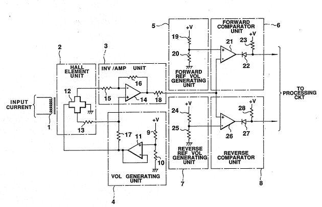
Fig. 1 is a circuit diagram illustrating an embodiment
of a current sensor circuit in accordance with the present
; invention.
~ The current sensor circuit shown in this diagram
;~ comprises a coil 1 for generating a magnetic flux of a
magnitude and a direction corresponding to a value and
direction of an input current; a Hall element unit 2 for
generating a Hall voltage corresponding to the magnitude and
direction of the magnetic flux produced by the coil 1; an ;~
inverter/amplifier unit 3 for amplifying the Hall voltage ~
output from the Hall element unit 2; and a voltage -
generating unit 4 for generating a voltage necessary for
effecting offset compensation for the inverter/amplifier
unit 3 and the driving of, and unbalance compensation for,
the Hall element unit 2.
The current sensor circuit further comprises a forward -~
reference voltage generating unit 5 for generating a forward
. .,
threshold voltage; a forward comparator unit 6 for
generating a ~ signal of a negative logic when the Hall
voltage output from the inverter/amplifier unit 3 is higher
: -:
than a forward threshold voltage output from the forward ~
' ~
' ~":'
~ ' ~ 4
- 8 - 20~3~
reference voltage generating unit 5; a reverse reference
voltage generating unit 7 for generating a reverse threshold
voltage; and a reverse comparator unit 8 for generating a
"1" signal of the negative logic when the Hall voltage
output from the inverter/amplifier unit 3 is lower than the
reverse threshold voltage output from the reverse reference :~
voltage generating unit 7.
: The coil 1 is inserted in an electric line which is an
object whose current is to be detected, and when a current
flows through this electric line, the coil 1 produces a
magnetic flux of a magnitude and a direction that correspond
to the magnitude and direction of that current.
The voltage generating unit 4 has two resistors 9, 10
for determining a reference voltage value, an operational
amplifier 11 for receiving the reference voltage value
determined by the values of these resistors 9, 10, and a
resistor 17 for transmitting an output voltage of this
operational amplifier 11 to the Hall element unit 2 and the
inverter/amplifier unit 3. The voltage generating unit 4
generates a reference voltage by causing the operational
~:
amplifier 11 to follow the reference voltage obtained by the
resistors 9, 10, supplies the same directly to a power input
. terminal of the Hall element unlt 2, and at the same time :
supplies the same to a compensation terminal of the Hall
.~.-
~`
~'
i,. ~
- 9 - Z03~3fi~ ;
element unit 2 and the inverter/amplifier unit 3 via the
resistor 17.
The Hall element unit 2 has a Hall element 12 which is ~:
magnetically connected to the aforementioned coil 1, as well
as a resistor 13 for compensating an unbalanced voltage of : .
the Hall element 12. When the reference voltage is supplied -:~
thereto from the voltage generating unit 4 via the power -
input terminal, the Hall element 12 is driven by this
reference voltage at a constant voltage, and the unbalanced :~
;~; lO voltage of the Hall element 12 is compensated by means of
the reference voltage input via the compensation terminal
and the resistor 13. In this state, when the coil 1
generates a magnetic flux, the Hall element 12 generates a ~. .
Hall voltage corresponding to the magnitude and direction of
the magnetic flux, and supplies the same to the .;
inverter/amplifier unit 3.
The inverter/amplifier unit 3 has an operational
: i amplifier 14 for effecting an amplifying operation, a
resistor 15 serving as an input resistor for the operational :
amplifier 14, a resistor 16 serving as a feedback resistor
for the operational amplifier 14, and a resistor 18 for
, ~
transmitting an output of the operational amplifier 14 to a
~: following-stage circuit, and an offset voltage of the
:-
operational amplifier 14 is compensated by the reference
voltage supplied from the voltage generating unit 4. In ;.
, ~:
, .~
. ,.. ",
-10- ~0~3fiS
addition, when the Hall voltage is supplied thereto from the
Hall element unit 2, the inverter/amplifier unit 3 inverts
and amplifies the same to generate an output voltage (Hall
voltage), and supplies the output voltage to the forward
comparator unit 6 and the reverse comparator unit 8.
The forward reference voltage generating unit 5 has
resistors 19, 20 for determining a forward threshold
voltage, and supplies the forward threshold voltage obtained
from the resistors 19, 20 to the forward comparator unit 6.
The forward comparator unit 6 has an operational
amplifier 21 for comparing the value of the forward
threshold voltage and the value of the Hall voltage output
from the inverter/amplifier unit 3, a diode 22 which is made
Y:
conductive when the output terminal of the operational
amplifier 21 assumes a low voltage, and a resistor 23 for
pulling up an anode of the diode 22. When the value of the
Hall voltage output from the inverter/amplifier unit 3 is
higher than the value of the forward threshold voltage, the
voltage at the output terminal of the operational amplifier
: 20 21 is set to a low level. As a result, the diode 22 is made
conductive, thereby allowing a "1" signal of the negative
logic to be generated and supplied to a following-stage
processing circuit (not illustrated).
The reverse reference voltage generating unit 7 has
resistors 24, 25 for determining a reverse threshold
.. ~i :
`:~
2~3~3
voltage, and supplies the reverse threshold voltage obtained
from these resistors 24, 25 to the reverse comparator unit ~-~
8.
In the same way as the forward comparator unit 6, the
reverse comparator unit 8 has an operational amplifier 26, a
diode 27, and a resistor 28 for pulling-up. When the value
of the Hall voltage output from the inverter/amplifier unit `;-~
3 is lower than the value of the reverse threshold voltage,
. .: ,: the voltage at the output terminal of the operational
amplifier 26 is set to a low level to make the diode 27 -
conductive, with the result that a "1" signal of the
negative logic is generated and supplied to the ;-
aforementioned processing circuit.
Thus, in this embodiment, since the constant-voltage
driving of the Hall element 12, the compensation of the
unbalance of the Hall element 12, and the compensation of
the offset of the operational amplifier 14 are effected by
means of the reference voltage generated by the voltage
generating unit 4, it is possible to reduce the number of
~1:: . :
parts used as compared with a conventional current sensor
circuit. In consequence, it is possible to attain a cost
reduction, high precision, and space saving of the circuit.
In addition, since in the above-described embodiment
the forward reference voltage generating unit 5 and the ;
reverse reference voltage generating unit 7 are formed
. ..
.~
:`
203~3~
-12-
independently, it is possible to make adjustment
: individually for the forward threshold voltage and the
reverse threshold voltage, with the result that it is
possible to effect high precision of the circuit and
facilitate adjustment.
INDUSTRIAL APPLICABILITY
' The current sensor circuit in accordance with the
present invention is employed for detecting the presence or
absence of a loop current in a communication line used for
lOfacsimile equipment, modems, and the like, and effects
. control and processing of the line on the basis of the:
result of detection.
~ ':
~' '
:
:~ ,'.
. ~
1:
. ~
. ~: