Note : Les descriptions sont présentées dans la langue officielle dans laquelle elles ont été soumises.
2034620
The present invention relates to a charge or
charging device for charging a storage cell.
A conventional charge device has a storage cell
terminal for connection to the storage cell, a trickle
charge terminal for receiving a trickle charge voltage of a
power supply, a boost charge terminal connected to the
storage cell terminal for receiving a boost charge voltage
of a boost charge circuit, and a constant current circuit
connected between the storage cell terminal and the trickle
charge terminal for causing a constant current to flow from
the trickle charge terminal to the storage cell terminal.
In the conventional charge device, the boost charge
circuit includes a charge completion detector for detecting
a change in a terminal voltage of the storage cell to
produce a charge completion signal when the change becomes
larger than a reference level. In the conventional charge
device, both the boost charge voltage and the trickle charge
voltage are supplied to the storage cell. Inasmuch as the
boost charge circuit charges the storage cell while the
storage cell is supplied with the trickle charge voltage,
the rate of the change of the terminal voltage becomes
slower. The charge completion detector detects the slow
rate of charge. As a result, the storage cell is charged
too much and the lifetime of the storage cell becomes
shorter.
It is therefore an object of the present invention
to provide a charge device which is capable of lengthening
the lifetime of the storage cell.
According to one aspect of the present invention,
there is provided a charge device comprising a storage cell
terminal adapted for connection to a storage cell to be
charged; a trickle charge terminal for receiving a trickle
charge voltage; a boost charge terminal connected to said
storage cell terminal for receiving a boost charge voltage;
a constant current circuit connected between said storage
cell terminal and said trickle charge terminal for causing
a constant current to flow from said trickle charge terminal
A ~
20346~0
to said storage cell terminal; boost charge detector means
connected to said boost charge terminal for detecting said
boost charge voltage to produce a boost charge signal when
said boost charge terminal is supplied with said boost
charge voltage; and interrupting means connected to said
boost charge detector means and said constant current
circuit for interrupting said constant current when said
boost charge detector means produces said boost charge
signal.
According to another aspect of the present
invention, there is provided a charge device comprising
charging means for charging a storage cell with a trickle
voltage; terminal means for receiving and applying a boost
voltage to said storage cell, said boost voltage being
higher than said trickle voltage; means for detecting when
said storage cell is being charged with said boost voltage,
and for producing a detection signal in response thereto;
and means responsive to said detection signal for
interrupting the charging of said storage cell by said
charging means.
According to a further aspect of the present
invention, there is provided a method for charging a storage
cell, comprising the steps of charging said storage cell
with a first voltage; charging said storage cell with a
second voltage higher than said first voltage; detecting
said storage cell being charged with said second voltage to
produce a detection signal; and responsive to said detection
signal, interrupting the charging of said storage cell with
said first voltage.
In the accompanying drawings which illustrate
embodiments of the present invention:
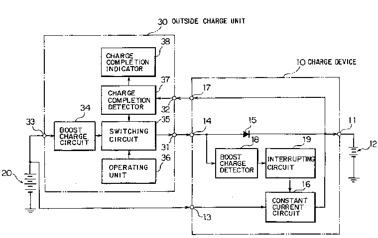
Figure 1 is a block diagram of a charge device
according to an embodiment of the present invention; and
Figure 2 is a circuit diagram of the charge device
illustrated in Figure 1.
Referring to Figure 1, a charge device 10 according
to a preferred embodiment of this invention has a storage
~ 2034620
cell terminal 11 for connection to a storage cell 12 to be
charged, a trickle charge terminal 13 for receiving a
trickle charge voltage, and a boost charge terminal 14
connected through a diode 15 to the storage cell terminal 11
for receiving a boost charge voltage which will presently be
described. A constant current circuit 16 is connected
between the storage cell terminal 11 and the trickle charge
terminal 13 for causing a constant current to flow from the
trickle charge terminal 13 to the storage cell terminal 11.
The charge device 10 furthermore has a charge detecting
terminal 17 connected to the storage cell terminal 11.
The charge device 10 comprises a boost charge
detector 18 connected to the boost charge terminal 14 for
detecting the boost charge voltage to produce a boost charge
signal when the boost charge terminal 14 is supplied with
the boost charge voltage. An interrupting circuit 19 is
connected to the boost charge detector 18 and the constant
current circuit 16 for interrupting the constant current
when the boost charge detector 18 produces the boost charge
signal.
The trickle charge terminal 13 is connected to a
power supply 20 which may include a vehicle battery and is
supplied with a supply voltage of the power supply 20 as the
trickle charge voltage. The boost charge terminal 14 and
the charge detecting terminal 17 are connected to a boost
charge output terminal 31 and a charge detecting voltage
input terminal 32 of an outside charge unit 30. The outside
charge unit 30 is connected through a boost charge input
terminal 33 to the power supply 20. The outside charge unit
30 may be employed to miniaturize and to reduce the weight
of the charge device 10.
The outside charge unit 30 includes a boost charge
circuit 34 connected to the boost input terminal 33, a
switching circuit 35 connected between the boost charge
circuit 34 and the boost charge output terminal 31, an
operating unit 36 connected to the switching circuit 35 for
producing a start signal, a charge completion detector 37
-- 203~620
connected between the switching circuit 35 and the charge
detecting voltage input terminal 32, and a charge completion
indicator 38 connected to the charge completion detector 37.
The boost charge circuit 34 is supplied with the
supply voltage of the power supply 20 to produce the boost
charge voltage having a voltage level which is higher than
a voltage level of a terminal voltage of the storage cell
12. The switching circuit 35 turns on when the switching
circuit 35 is supplied with the start signal from the
operating unit 36 and turns off when the switching circuit
35 is supplied with a charge completion signal from the
charge completion detector 37. While the switching circuit
35 is on, the boost charge terminal 14 is supplied with the
boost charge voltage from the boost charge circuit 34
through the switching circuit 35 and the boost charge output
terminal 31.
The charge completion detector 37 is supplied with
the terminal voltage of the storage cell 12 through the
storage cell terminal 11, the charge detecting terminal 17,
and the charge detecting voltage input terminal 32. The
charge completion detector 37 detects a change in the
terminal voltage of the storage cell 12 to produce the
charge completion signal in response to a completion of a
charge of the storage cell 12 when the change of the
terminal voltage is larger than a reference level. The
charge completion indicator 38 is supplied with the charge
completion signal to indicate the completion of the charge
of the storage cell 12. The charge completion detector 37
may be similar to a charge detecting circuit disclosed in
the co-pending application which claims priority from
Japanese Patent Application No. 171988/1989.
Referring now to Figure 2, the charge device 10
will be described more in detail. The constant current
circuit 16 comprises a first transistor 161 which has a
collector electrode connected to the trickle charge terminal
13. A second transistor 162 has a base electrode connected
to an emitter electrode of the first transistor 161, a
.
2034620
collector electrode connected to a base electrode of the
first transistor 161, and an emitter electrode connected to
the storage cell terminal 11. A first resistor 165 is
connected between the collector and the base electrodes of
the first transistor 161. A second resistor 166 is
connected between the base and the emitter electrodes of the
second transistor 162.
In the constant current circuit 16, a resistor
current in the second resistor 166 becomes larger when an
internal resistance of the storage cell 12 becomes smaller.
A resistor voltage across the second resistor 166 becomes
higher and an internal resistance of the second transistor
162 becomes smaller. As a result, a base voltage of the
base electrode of the first transistor 161 becomes lower and
an internal resistance of the first transistor 161 becomes
larger. Therefore, the constant current circuit 16 causes
the constant current to flow from the trickle charge
terminal 13 to the storage cell terminal 11.
In the constant current circuit 16, the resistor
current in the second resistor 166 becomes smaller when the
internal resistance of the storage cell 12 becomes larger.
The resistor voltage across the second resistor 166 becomes
lower and the internal resistance of the second transistor
162 becomes larger. As a result, the base voltage of the
base electrode of the first transistor 161 becomes higher
and the internal resistance of the first transistor 161
becomes smaller. Therefore, the constant current circuit 16
causes the constant current to flow from the trickle charge
terminal 13 to the storage cell terminal 11.
The constant current circuit 16 is supplied with
the supply voltage of the power supply 20 (shown in Figure
1) as the trickle charge voltage through the trickle charge
terminal 13 to supply the constant current to the storage
cell terminal 11.
The boost charge detector 18 has a third transistor
181 which has an emitter electrode connected to ground and
a base electrode connected through a resistor 182 to the
` 2034620
boost charge terminal 14. The interrupting circuit 19 has
a conductor 191 connected between a collector electrode of
the third transistor 181 and a point of connection between
the base electrodes of the first transistor 161 and the
collector electrode of the second transistor 162.
Inasmuch as the third transistor 181 assumes an on
state when the boost charge terminal 14 is supplied with the
boost charge voltage, the base electrode of the first
transistor 161 is connected to ground through the conductor
191 and the third transistor 181. As a result, the first
transistor 161 assumes an off state. Therefore, the
constant current in the constant current circuit 16 is
interrupted. While the boost charge terminal 11 is supplied
with the boost charge voltage, the storage cell 12 is
supplied only with the boost charge voltage, that is, the
storage cell 12 is not supplied with the constant current
which would otherwise be supplied from the constant current
circuit 16 in response to the trickle charge voltage.
A