Note : Les descriptions sont présentées dans la langue officielle dans laquelle elles ont été soumises.
204 1 942
QUANTUM WIRE FABRICATED VIA PHOTO
INDUCED EVAPORATION ENHANCEMENT
DURING IN SITU EPITAXIAL GROWTH
Cross-Reference to Related Patents
This application contains subject matter that is
related to the subject matter of U. S. Patents 4,962,057
and 5,013,684.
Background of the Invention
The present invention relates generally to semi-
conductor structures and more particularly to semi-
conductor structures having quantum wires fabricated
employing in situ photo induced modifications to compound
semiconductor films during epitaxial growth.
The hallmark of the electronics industry has been
miniaturized. The size required for computer chips and
semiconductors has plunged nearly a thousand-fold in just
ten years. The future suggests even further progress in
shrinking electronic elements.
One aspect of the semiconductor has not kept pace in
this rush toward miniaturization, the wires carrying the
electric current flow to and from the ever smaller
lasers, p-n junctions, transistors, LEDs and other
diodes, detectors, integrated circuits, microelectronics
and the like. This may eventually lead to the rather
incongruous sight of the wiring connecting circuitry
components being larger than the components themselves.
Quantum wires in semiconductors are regions in which
the charge carriers are quantum confined in the 2
dimensions orthogonal to the axis of the wire. Quantum
effects in GaAs layers are most strong when the thickness
is less than 50 nm. A ~
-1- .~'
r ;,~ ¦
,
~t~l9~2
quantum wire will still be useful if only one of its dimensions is less than 50 nm. For
GaAs this typically means a region for the quantum wire in a semiconductor smaller
than about 50 nm by 100 nm.
In addition to their current conductance, quantum wires are expected to have
useful and novel electrical properties such as extremely high electron mobility due to
the two dimensional confinement of carriers. Quantum wires of the appropriate
size are expected to act like electron waveguides which are analogous to opticalwaveguides.
In situ fabrication of arrays of quantum wires has been contemplated and
demonstrated by Fukui et al., n(AlAs)o 5 (GaAs)o s fractional-layer superlattices
grown on (001) vicinal surfaces by metalorganic chemical vapor deposition" in Appl.
Phys. Letters 50, 824 (1987) and Tsuchiya et al. in Phys Rev Letters 62, 466 (1989)
using stepped surfaces obtained with off axis substrates to produce tilted
superlattices. A difficulty with this approach is the propagation of this surface
topography through the relatively thick layers required for the other layers of a
semiconductor structure. Also, the resulting poor geometry of the quantum wires in
the structure would make them ineffective as current carrying wires.
What is desired is a process, particularly as implemented in molecular beam
epitaxy (MBE) or metalorganic chemical vapor deposition (MOCVD), wherein
ultrafine patterning of conducting channels or wires or electron waveguides can be
achieved in situ without growth interruption by some off-line or nongrowth
procedure or process.
There are two examples known to us where patterning may be achieved by quasi-
in situ thermal processing wherein thermal etching is employed to selectively
remove GaAs. In one example, a n-GaAs layer over a p-AlGaAs layer is first,
selectively chemically etched in a particular region followed by thermal etching to
remove the remaining thin GaAs left from chemical etching before proceeding withregrovvth of the p-AlGaAs layer. This forms a buried reverse biased current
confinement mechanism in a double heterostructure laser. H. Tanaka et al, nSingle-
Longitudinal-Mode Self Aligned AlGa~As)Double-Heterostructure Lasers Fabricated
by Molecular Beam Epitaxyn, Japanese Journal of Applied Physics, Vol. 24, pp. L89-
L90, 1985.
204 1 942
In the other example, a GaAs/AIGaAs heterostructure
partially masked by a metallic film is thermally etched
in an anisotropic manner illustrating submicron
capabilities for device fabrication. A.C. Warren et al,
"Masked, Anisotropic Thermal Etching and Regrowth for in
Situ Patterning of Compound Semiconductors", applied
Physics Letters, Vol. 51 (22), pp. 1818-1820, November
30, 1987. In both of these examples, AIGaAs masking
layers are recognized as an etch stop to provide for the
desired geometric configuration in thermally etched GaAs,
although it is also known that, given the proper
desorption parameters, AIGaAs may also be thermally
etched at higher temperatures with different attending
ambient conditions vis-a-vis GaAs.
However, none of these techniques employ in situ
photo induced evaporation as a technique in a film
deposition system to incrementally reduce, on a minute
scale, film thickness in patterned or selective locations
at the growth surface either during or after film growth,
producing smooth sculptured surface morphology which is a
principal objective of this invention.
It is an object of an aspect of this invention to
bring about in situ removal or desorption of selected
surface regions or layers of compound semiconductors
employing induced evaporation enhancement in metalorganic
chemical vapor deposition (MOCVD) epitaxy and to apply
this method in the fabrication of in situ fabricated
quantum wire in a semiconductor structure.
It is an object of an aspect of this invention to
fabricate a quantum wire layer in a groove of a
semiconductor structure and to eliminate the side regions
of a deposited quantum well layer in the groove and
adjust the lateral dimensions of the quantum well layer
to form the quantum wire.
P~
204 1 942
It is an object of an aspect of this invention to
fabricate patterned quantum wire and multiple quantum
wire layers, both horizontally or vertically, or in a
two-dimensional array of a semiconductor structure.
Summary of the Invention
According to this invention, in situ removal or
thinning of portions or all of selected regions of
deposited films are brought about by a technique
employing an irradiation energy source directed to a spot
or region of exposure on the growth surface of a
substrate or support in a deposition system, e.g., MBE or
MOCVD system. This technique, termed "induced
evaporation enhancement", is taught in U. S. Patent
4,962,057.-
In particular, the invention herein is directed to
the employment of this technique in fabricating in situ
quantum wires in semiconductor structures wherein induced
evaporation enhancement purely removes or prevents the
continued growth of the epitaxially deposited materials
in selected regions at the growth surface without theneed or introduction of masking or chemical etching
processes.
Other aspects of this invention are as follows:
A method of forming a quantum wire in a semi-
conductor structure comprising the steps of: epitaxially
depositing a quantum well layer on a semiconductor layer
or substrate, said semiconductor layer or said substrate
having a groove, interrupting the epitaxial growth after
the deposition of said quantum well layer, selectively
desorbing in situ, employing photo induced evaporation,
portions of said quantum well layer in said groove to the
interface with the layer therebeneath leaving a quantum
wire in the vertex of said groove, and epitaxially
depositing at least one semiconductor layer upon said
quantum wire, said groove and said semiconductor layer or
said substrate.
--4--
204 1 94~
A semiconductor structure with a quantum wire
comprising: a substrate or a semiconductor layer,
a groove in said substrate or semiconductor layer,
a quantum wire at the vertex of said groove, and
a semiconductor layer on said quantum wire and said
groove and said substrate or semiconductor layer.
A method of forming a patterned quantum wire in a
semiconductor structure comprising the steps of: forming
a patterned groove in a semiconductor layer or a
lo substrate, epitaxially depositing a quantum well layer on
said semiconductor layer or said substrate, interrupting
the epitaxial growth after the deposition of said quantum
well layer, selectively desorbing in situ, employing
photo induced evaporation, portions of said quantum well
layer in said patterned groove to the interface with the
layer therebeneath leaving a quantum wire in the vertex
of said patterned groove, and epitaxially depositing at
least one semiconductor layer upon said quantum wire,
said patterned groove and said semiconductor layer or
said substrate.
A semiconductor structure with a patterned quantum
wire comprising: a substrate or a semiconductor layer,
a patterned groove in said substrate or semiconductor
layer, a quantum wire at the vertex of said patterned
groove, and a semiconductor layer on said quantum wire
and said patterned groove and said substrate or semi-
conductor layer.
A method of forming multiple quantum wires in a
semiconductor structure comprising the steps of:
epitaxially depositing a quantum well layer on a
semiconductor layer or a substrate, said semiconductor
layer or said substrate having a series of grooves,
interrupting the epitaxial growth after the deposition of
said quantum well layer, selectively desorbing in situ,
employing photo induced evaporation, portions of said
quantum well layer in said grooves to the interface with
-4a-
204 1 942
the layer therebeneath leaving a quantum wire in thevertex of each of said series of grooves, and
epitaxially depositing at least one semiconductor layer
upon said quantum wires, said series of grooves and said
semiconductor layer or said substrate.
A semiconductor structure with multiple quantum
wires comprising: a semiconductor layer or a substrate,
a series of grooves in said semiconductor layer or said
substrate,a quantum wire at the vertex of each of said
series of grooves, and a semiconductor layer on said
quantum wires and said series of grooves and said
semiconductor layer or said substrate.
A method of forming multiple quantum wires in a
semiconductor structure comprising the steps of:
epitaxially depositing a quantum well layer on a
semiconductor layer or a substrate, said semiconductor
layer or said substrate having a groove interrupting the
epitaxial growth after the deposition of said quantum
well layer, selectively desorbing in situ, employing
photo induced evaporation, portions of said quantum well
layer in said groove to the interface with the layer
therebeneath leaving a quantum wire in the vertex of said
groove, epitaxially depositing a barrier layer, forming a
groove in said barrier layer, epitaxially depositing a
quantum well layer on said barrier layer, interrupting
the epitaxial growth after the deposition of said quantum
well layer, selectively desorbing in situ, employing
photo induced evaporation, portions of said quantum well
layer in said groove in said barrier layer to the
interface with the layer therebeneath leaving a quantum
wire in the vertex of said groove, and epitaxially
depositing at least one semiconductor layer upon said
quantum wire, said groove and said barrier layer.
A semiconductor structure with multiple quantum wire
comprising: a semiconductor layer or a substrate, a
groove in said semiconductor layer or said substrate, a
-4b-
B
204 1 942
quantum wire at the vertex of said groove, a barrierlayer having a groove, a quantum wire at the vertex of
said groove in said barrier layer, and a semiconductor
layer on said quantum wire and said groove and said
barrier layer.
A method of connecting multiple quantum wires in a
semiconductor structure comprising the steps of:
epitaxially depositing a quantum well layer on a
semiconductor layer or a substrate, said semiconductor
layer or said substrate having a groove, interrupting the
epitaxial growth after the deposition of said quantum
well layer, selectively desorbing in situ, employing
photo induced evaporation, portions of said quantum well
layer in said groove to the interface with the layer
therebeneath leaving a quantum wire in the vertex of said
groove, epitaxially depositing a barrier layer, forming a
groove in said barrier layer, fabricating a hole in said
groove in said barrier layer to said quantum wire,
epitaxially depositing a quantum well layer on said
barrier layer and in said hole, interrupting the
epitaxial growth after the deposition of said quantum
well layer, selectively desorbing in situ, employing
photo induced evaporation, portions of said quantum well
layer in said groove in said barrier layer to the
interface with the layer therebeneath leaving a quantum
wire in the vertex of said groove and a quantum wire in
said hole connecting said quantum wires in said grooves,
and epitaxially depositing at least one semiconductor
layer upon said quantum wires, said groove and said
barrier layer.
A semiconductor structure with connected quantum
wires comprising: a semiconductor layer or a substrate,
a groove in said semiconductor layer or said substrate,
a quantum wire at the vertex of said groove, a barrier
layer having a groove and a hole to said quantum wire in
said semiconductor layer or said substrate, a quantum
-4c-
F~ '
~4 ~ 942
wire at the vertex of said groove in said barrier layer,a quantum wire in said hole connecting said quantum wires
in said grooves, and a semiconductor layer on said
quantum wire in said groove in said barrier layer and
said groove and said barrier layer.
Other objects and attainments together with a fuller
understanding of the invention will become apparent and
appreciated by referring to the following description and
claims taken in conjunction with the accompanying
drawings.
Brief Description of the Drawings
Figure 1 is a schematic illustration of a side elevation
of a quantum wire semiconductor structure prior to photo
induced desorption formed according to this invention.
Figure 2 is a schematic illustration of a side elevation
of a quantum wire semiconductor structure during photo
induced desorption formed according to this invention.
Figure 3 is a schematic illustration of a side elevation
of a quantum wire semiconductor structure formed
according to this invention.
Figure 4 is a schematic illustration of a top elevation
of patterns of quantum wire semiconductor structure
formed according to this invention.
Figure 5 is a schematic illustration of a side elevation
of a series of linear or horizontal multiple quantum wire
semiconductor structure formed according to this
invention.
Figure 6 is a schematic illustration of a side elevation
of a vertical series of linear or horizontal quantum wire
semiconductor structure formed according to this
invention.
-4d-
. .~. "
4 2
Figure 7 is a schematic illustration of a side elevation of an alternative embodin~ent
of a verticai series of linear or horizontai quantum wire semiconductor struc~ure
formed according to this invention.
Figure 8 is a schematic illustration of a cut-away side elevation of a vertical quantum
wiresemiconductorstructure priorto photo induced desorption formed according
to this invention.
Figure 9 is a schematic illustration of a cut-away side elevation of a vertical quantum
wire semiconductor structure during photo induced desorption formed according tothis invention.
Figure 10 is a schematic illustration of a cut-away side elevation of a verticalquantum wire semiconductor structure formed according to this invention.
Description of the Preferred Embodiments
In describing the devices of this invention, reference is generally made to
individual discrete structures although it is generally the case that a plurality of such
devices would be fabricated on a wafer substrate in a MOCVD reactor wherein the
processing laser beam would be scanned and/or modulated to selected locations toperform the desired induced evaporation enhancement in patterned fashion across
the wafer surface.
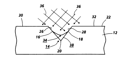
Reference is now made to Figure 1 wherein there is disclosed
a semiconductor structure 10 having a single quantum wire and
fabricated using MOCVD processing as described in U.S. Patent
4,962,057. Semiconductor structure 10 includes a semiconductor
cladding layer or substrate 12 of high bandgap semiconductor
material such as AlxGa1xAs upon which is formed a groove 14. If
a semiconductor cladding layer is used, the layer can be anywhere
in a semiconductor structure.
The groove can be fabricated in the cladding layer by chem-
ical etching, reactive ion etching, ion milling or other means
known to those of ordinary skill in the art. The groove can also
be fabricated by a tightly focussed beam scanned across the
,~
.~ ~
204 ~
,urface of the cladding layer with changing dwell time, a process
described in U.S. Patent 4,962,057.
In general, the groove should be as narrow as possible. However, the width and
depth of the groove will depend upon the process used to fabricate it. For example,
chemical etching and beam desorption form grooves that are wider than their
depth. It is desirable to form grooves which are deeper than their width with
sidewall angles greater than 45 degrees. Reactive ion etching or ion milling form
grooves with greater than 45 degrees sidewalls and even grooves with vertical
sidewalls.
For the sake of illustration in this embodiment, the groove 14 is V-shaped with
opposing angled sidewalls 16 and 18 culminating in vertex 20. The groove can be
from 10 nm to 2.5 microns deep.
Upon the cladding layer 12, a quantum well layer 22 of low bandgap
semiconductor material such as GaAs or AI~Ga1 2As where z < x is grown at a
temperature greater than 725 C. The quantum well layer is typically less than 30 nm
thick. A groove 24 in the quantum well layer is formed in the groove 14 in the
cladding layer. The growth rate on the sidewalls 26 and 28 of the groove 24 of the
quantum well layer at this temperature is lower than on the horizontal top surfaces,
or mesas, 30 and 32, allowing formation of a slightly thicker region 34 at the vertex
of the quantum well groove as shown in Figure 1.
Upon completion of the growth of quantum well layer 22,
however, epitaxial growth is temporally discontinued, and as
taught in U.S. Patent 4,962,057, the trimethyl-gallium (TMG)
source to the MOCVD chamber is turned off, the substrate
temperature is increased to about 825C and a laser beam or
combination laser beam is focussed on the surface of quantum well
layer 22 either orthogonally or, as indicated by lines 36 in
Figure 2, at an angle near normal incidence to the sidewalls for
a period of time sufficient to thermally evaporate quantum well
layer 22 at sidewalls 26 and 28 to the sidewalls 16 and 18 of
cladding layer 12 at a rate of 1 A/second. The temperature at
the illuminated portion of the quantum layer 22 during the
evaporation process may be about 1000C to 1030C.
It is well known in the art that at temperatures above about
725C the growth of GaAs on sidewalls of a mesa or groove is
slower than on the mesa top or at the
.. ~
~o~
vertex of the groove and that the difference increases tU rtner as t~e temperatu re lS
increased. This behavior implies that the sticking coefficient for Ga and As atoms lS
smallest on the sidewalls. Hence for near normal incidence of the optical
illumination increased temperature is expected to desorb the GaAs of quantum well
layer 22 preferentially from the sidewalls 26 and 28 and the top mesa areas 30 and
32 of the quantum well layer 22 compared to the region 34 at the vertex 20 of the
quantum well groove 24.
By controlling the illumination intensity, the angle and the length of exposure of
the laser beam 36, the areas of quantum well layer 22 along the sidewalls 26 and 28
are desorbed down to the interface with cladding layer 12 resulting in a crescent
shaped quantum wire 38 forming in the vertex 2û of the groove 14 of the claddinglayer 12. The AIxGa1 xAs of the cladding layer 12 functions as a desorption stop to
the optically induced desorption because AIxGa1 xAs where x ~ 0.15 is much more
difficult to desorb according to this process as compared to the desorption of the
GaAs of the quantum well layer 22.
In any case, the operating temperature for AlGaAs will be higher than that for
GaAs because the Al content in AlGaAs causes a slower evaporation rate since GaAs
has a higher vapor pressure than AlGaAs.
The incident angle of the laser beam 36 can also be adjusted to shadow the
vertex and concentrate illumination on the sidewalls as shown in Figure 2. The
desorption of the quantum well layer in the shadowed vertex region will proceed
more slowly than it would in the presence of illumination since any photochemical
desorption will be reduced or eliminated and the vertex region will be cooler than its
surrounding sidewalls. Both effects will enhance the lateral selectivity of the
desorption. The optical process should be highly reproducible because exposure time
and illumination intensity can be accurately controlled.
The method of U.S. Patent 4,962,057 allows growth of the
quantum well layer to be performed at a temperature that
optimizes the quality of the layer for the flow of electrical
current. The desorption can subsequently be accomplished at a
base temperature conducive to the preferential thinning of the
sidewalls relative to the vertex region. The laser approach to
the desorption is preferable to the simple raising of the
temperature of the substrate to induce
4 ~
desorption because the intensity of the optical illumination allows for faster control
of the semiconductor temperature, shorter desorption times and less time s,oent at
high undesired temperatures. All of these factors greatly enhance the
reproducibility of the process using optical illumination.
As shown in Figure 3, after photo-induced desorption, a crescent shaped
quantum wire 38 has formed in vertex 20 of the groove 14 of the cladding layer 12
with the quantum well layer no longer existing on the sidewalls of the groove or the
mesa levels on top of the cladding layer. Epitaxial growth is then continued with the
growth of a cladding layer 40 of high bandgap semiconductor material such as
AlyGa1 yAs where y>z and x>z, but y can be > or < x . The semiconductor claddinglayer 40 can either follow the contour of the previously deposited cladding layer 12
with its groove 14 and crescent shaped quantum wire 38 or, as shown in this Figure,
provide a flat upper surface 42. Other semiconductor layers can be deposited on
cladding layer 40.
One alternative to having a lower bandgap material quantum wire between
higher bandgap material cladding layers is to have the quantum wire of doped
material and the cladding layers of undoped or semi-insulating material. The initial
cladding layer 12 of Figures 1 to 3 would be a layer of undoped or p-AIxGa1 xAs. The
quantum well layer 22 of Figure 1 would be a n-type doped quantum well layer
comprising n-GaAs heavily doped, for example, with Si or Se at a concentration of
1019/cm3. The quantum well layerwould be desorbed down to form the quantum
wire 38 of Figures 2 and 3 and a cladding layer 40 of undoped or p-AIxGal xAs would
be grown on top of the quantum wire, as shown in Figure 3.
The doping content of the quantum well layer is of opposing conductivity type tothe adjacent undoped or semi-insulating cladding layers. Thus, the quantum wire
and the cladding layers can be of the same material, for example AlGaAs, even
though the bandgap would obviously be the same for both the wire and the
cladding.
By patterning the length and direction of the groove in the cladding layer as
shown in Figure 4, quantum wires cari be f~rmed at a right angle 44, a curve 46, a Y-
branch 48, a T-branch 50 or any other pattern useful for the flow of electric current
or electronic circuitry or electronic waveguides. Curves may require special etching
techniques.
Figure 5 discloses a semiconductor structure 52 with a series of linear or
horizontal multiple quantum wires. The semiconductor structure 52 includes a
semiconductor cladding layer or substrate 54 of GaAs or AIxGal xAs~ upon which
multiple grooves 56 have been fabricated. Upon the cladding layer and grooves isepitaxially deposited a quantum well layer of GaAs or AIzGal zAs where zc x which
is desorbed down to crescent shaped quantum wires 58 in the vertices of the
grooves by means previously taught in this application. The desorbing laser beamcan either be a single laser beam or a combination beam working in sequence, or
more appropriately, multiple laser beams or combination laser beams working in
parailel or in series. A semiconductor cladding layer 60 of AlyGal.yAs is epitaxially
deposited on top of the exposed surfaces of the semiconductor layer 54, the grooves
56 and the quantum wires 58 also as previously taught in this application. It is not
necessary that the grooves, and thus the quantum wires, be parallel. As discussed
with regard to Figure 4, patterns can be formed.
Figure 6 discloses a semiconductor structure 62 with a vertical series of linear or
horizontal quantum wires. The semiconductor structure 62 includes a
semiconductor cladding layer or substrate 64 of GaAs or AIxGal xAsl upon which a groove 66 has been fabricated. Upon the cladding layer and groove is epitaxially
deposited a quantum well layer of GaAs or AIzGa1 zAs where z< x which is
desorbed down to a crescent shaped quantum wire 68 at the vertex of the groove by
means previously taught in this application. A barrier layer 70 of high bandgap
semiconductor material such as AIcGa1 cAs where z<c is then epitaxially deposited
over the exposed surfaces of the semiconductor layer 64, the groove 66 and the
quantum wire 68. The barrier layer follows the contour of the previously deposited
layer, groove and quantum wire to form a groove 72 in its surface, spatially aligned
vertically with the groove 66 in the semiconductor layer 64.
Another quantum well layer is grown on top of the barrier layer 70 and photo
induced desorbed by means previously taught in this application leaving a crescent
shaped quantum wire 74 at the vertex of t~e groove 72.
Another barrier layer 76 is deposited, followed by a quantum well layer which isdesorbed to leave a crescent shaped quantum wire 78 at the vertex of a groove 80.
204 1 94%
EDitaxial growth is then continued with the gro~h of a semiconductor cladding
layer 82 of AlyGal.yAs which can either follow the contour of the previously
deposited barrier layer 76 with its groove 80 and crescent shaped quantum wire 78
or, as shown in this Figure, provide a flat upper surface 84.
In this Figure, the barrier layer follows the contour of the previous cladding or
barrier layer. Thus, since there is a groove in the cladding layer, an aligned groove
will form in the barrier layer when the barrier layer is epitaxially deposited on top of
the cladding layer.
If the barrier layer is grown with a flat upper surface, the groove in
the barrier layer can also be fabricated by the same means as the groove in
the cladding layer, namely by chemical etching, reactive ion etching, ion
milling or other means known to those of ordinary skill in the art. The
groove can also be fabricated by a tightly focussed beam scanned across the
surface of the cladding layer with changing dwell time, a process described in
U.S. Patent 4,962,057.
One alternative to having the high bandgap semiconductor material barrier layer
is to have the quantum wire of doped material and the cladding layers and barrier
layers of undoped or semi-insulating material. The initial cladding layer 64 of Figure
6 would be a layer of undoped or p-AIxGa1 xAs. The quantum well layer and the
resulting quantum wire 68 would be a n-type doped quantum well layer comprising
n-GaAs heavily doped, for example, with Si or Se at a concentration of 1019/cm3. The
barrier layer 70 of undoped or p-AIxGa1 xAs would be grown on top of the quantumwire. The other barrier layers 70 and 76 and the semiconductor cladding layer 82would also be undoped or p-AIxGa1 xAs and the other quantum wires 74 and 78
would be heavily doped n-GaAs.
The doping content of the quantum well layer is of opposing conductivity type tothe adjacent undoped or semi-insulating cladding and barrier layers. Thus, the
quantum wire and the cladding and barrier layers can be of the same material, for
example AlGaAs, even though the bandgap would obviously be the same for both
the wire and the cladding.
The sequentially grown quantum wires of Figure 6 are all self-aligned by the
formation of the grooves. This growth sequence of alternating barrier layers andquantum well layers to be desorbed into quantum wires in the vertex of a groove of
--10--
.. . .
the barrier layer can be repeated to form as many quantum wires and layers of
quantum wires as desired to form a multi-line bus of quantum wires buried in thesemiconductor.
Alternatively, as shown in Figure 7, the quantum wires of a semiconductor
structure need not be aligned, but can cross spatially separated by a barrier layer.
The semiconductor structure 84 with multiple vertical quantum wires includes a~
semiconductor cladding layer or substrate 86 of GaAs or AIxGa1 xAs, upon which agroove 88 has been fabricated by means previously discussed in this application.Upon the cladding layer and groove is epitaxially deposited a quantum well layer of
GaAs or AIzGal zAs where z< x which is desorbed down to a crescent shaped
quantum wire 90 at the vertex of the groove by means previously taught in this
application. A barrier layer 92 of AIcGal.cAs where z~c or any semi-insulating or
low bandgap semiconductor material is then epitaxially deposited over the exposed
surfaces of the semiconductor layer 86, the groove 88 and the quantum wire 90 toform a flat u pper surface 94 to the barrier layer.
A groove 96 is fabricated in the barrier layer 92 by means previously taught in this
application. The groove 96 in the barrier layer is not aligned with the groove 88 in
the cladding layer. Spatially, the grooves can be at any angle relative to each other.
For the purposes of this example, the groove 96 in the barrier layer is at right angles,
orthogonal to the groove 88 in the cladding layer.
Another quantum well layer is grown on top of the barrier layer 92 and photo
induced desorbed by means previously taught in this application leaving a crescent
shaped quantum wire 98 at the vertex of the groove 96.
As shown in the Figure, it is not necessary that the quantum wires be parallel and
the wires may cross spatially at any angle relative to each other, separated by the
barrier layer. This growth sequence of alternating depositing barrier layers, forming
grooves and depositing quantum well layers to be desorbed into quantum wires in
the vertex of a groove of the barrier layer can be repeated to form as many quantum
wires and layers of quantum wires and patterns of quantum wires as desired.
Epitaxial growth is then continued with the growth of a semiconductor cladding
layer 100 of AlyGa1 yAs which can either follow the contour of the previously
deposited barrier iayer 92 with its groove 96 and crescent shaped quantum wire 98
or, as shown in this figure, provide a flat upper surface 102.
Figure 8 discloses a semiconductor structure 104 with a vertical quantum wire.
Semiconductor structure 104 includes a semiconductor cladding layer or substrate106 of GaAs or AIxGa1 xAs~ upon which a groove 108 has been fabricated by means
previously discussed in this application. Upon the cladding layer and groove is
epitaxially deposited a quantum well layer of GaAs or AIzGal ~As where z~ x which
is desorbed down to a crescent shaped quantum wire 1 10 at the vertex of the groove
by means previously taught in this application. A barrier layer 112 of AIcGal cAs
where z<c or any semi-insulating or low bandgap semiconductor material is then
epitaxially deposited over the exposed surfaces of the semiconductor layer 106, the
groove 108 and the quantum wire 1 10 to form a flat upper surface 1 14 to the barrier
layer.
A groove 116 is fabricated in the barrier layer 112 by means previously taught in
this application. The groove 116 in the barrier layer is spatially orthogonal to the
groove 108 in the cladding layer. A hole 1 18 is fabricated vertically in the groove 1 16
through the barrier layer 112 to the buried quantum wire 110 in the groove 108 in
the cladding layer 106. This connecting hole can be fabricated by the same meanspreviously taught in this application as the grooves are fabricated. Similarly, the
connecting hole can be a shallow or deep groove or a groove with vertical walls.
Another quantum well layer is deposited on top of the barrier layer 1 12 to fill the
groove 116 and the connecting hole 118 as shown in Figure 9. The quantum well
layer is photo induced desorbed by means previously taught in this application
leaving a crescent shaped quantum wire 120 at the vertex of the groove 116 and ave~tical quantum wire 122 in the hole 118 connecting quantum wire 120 and
quantumwire 110.
Epitaxial growth is then continued, as shown in Figure 10, with the growth of a
semiconductor cladding layer 122 of AlyGa1 yAs which can either follow the contour
of the previously deposited barrier layer 1 12 with its groove 1 16 and crescent shaped
quantum wire 120 or, as shown in this-Figure, provide a flat upper surface 124.
2 ~
The horizontal quantum wires will be isolated from each other by the barrier
layer except for the connecting hole where the vertical quantum wire connects the
horizontal quantum wires.
The use of horizontal quantum wires in Figures 8 to 10 is for the purposes of
example. The quantum wires to be connected can be oriented at any angle spatially
relative to each other, even aligned as in Figure 6.
Alternatively, the connecting hole 118 can be filled with a quantum well layer of
a different semiconductor material to form the vertical quantum wire 122. The
quantum well layer deposited in the groove 116 and over the filled in connectinghole 118 and photo induced desorbed to form quantum wire 120 would be the same
material used to form quantum wire 110. This different semiconductor material for
the connecting quantum wire would have a lower bandgap than the semiconductor
material used to form the quantum wires 110 and 120. The lower bandgap would
aid in current flow through the connecting vertical quantum wire between the
horizontal quantum wires.
One alternative to having the high bandgap semiconductor material barrier layer
is to have the quantum wire of doped material and the cladding layers and barrier
layers of undoped or semi-insulating material. The initial cladding layer would be a
layer of undoped or p-AIxGal xAs. The quantum well layers and the resulting
quantum wires would be a n-type doped quantum well layer comprising n-GaAs
heavily doped, for example, with Si or Se at a concentration of 1019/cm3. The barrier
layers of undoped or p-Alx6al xAs would be grown on top of the quantum wire. Thevertical quantum wire could be even more heavily doped or of a different material
or a different dopant to aid in current flow through the connecting vertical
quantum wire between the horizontal quantum wires.
The doping content of the quantum well layer is of opposing conductivity type tothe adjacent undoped or semi-insulating cladding and barrier layers. Thus, the
quantum wire and the cladding and barrier layers can be of the same material, for
example AlGaAs, even though the bandgap would obviously be the same for both
the wire and the cladding. ~~
Alternatively, a semiconductor structure with a vertical quantum wire could be
fabricated by rotating the semiconductor structure 12 in Figures 1 to 3 by 90 degrees,
--13--
204 1 94~
either before or after formation of the quantum wire. Horizontal and vertical
quantum wlres can be formed in the same semiconauctor struure by rotating ~he
structure depending upon whether horizontal or vertical quantum wires are to be
fabricated. The ends of the quantum wires can be left open, not covered by the
barrier or cladding layers, so that the quantum wires can be connected.
Vertical and horizontal quantum wires could be fabricated together and
connected together for the purposes of circuitry or carrying electrical current.
The processing techniques in U.S. Patent 4,962,057 permit
the full in situ processing of a quantum wire without removal of
the semiconductor structure from the MOCVD reactor or movement or
masking of the structure in the reactor.
It naturally follows that multiple layers of horizontal, vertical and patterned
multiple quantum wires can be combined in a myriad of ways obvious to those of
skill in the art to form electronic circuitry or channels for current flow or to function
as electronic waveguides. The quantum wire can be formed anywhere within a
multi-layer semiconductor structure.
Although the foregoing discussion has been described in conne~tion with
semiconductors of GaAs and GaAlAs, other III-V alloys may be employed in the
practice of this invention, such as InGaP, ~nGaAsP, GaAlAsP, InGaAlP, InGaAlAsP, InP
or GaAlSb or Il-VI materials, e.g., ZnSe, ZnSSe and CdS. Also, Group IV materials,
most importantly Si and Ge, may be utilized as semiconductor layers or a multiple
quantum well structure of alternating well layers of GaAs or AI~Gal.~As and
corresponding barrierlayersofeitherAlAsorAl~Ga1.~Aswherex>y~z'>z. In a
multiple quantum wire semiconductor structure, different quantum wires can be ofdifferent quantum well semiconductor material depending upon circumstances and
needs.
While the invention has been described in conjunction with specific
embodiments, it is evident to those skilled in the art that many alternatives,
modifications and variations will be apparent in light of the foregoing description.
Accordingly, the invention is intended to embrace all such alternatives,
modifications and variations as fall within the spirit and scope of the appendedclalms.