Note : Les descriptions sont présentées dans la langue officielle dans laquelle elles ont été soumises.
CFO X838
- 1 -
2p 48470
PLASPSA PROCESSING APPARATUS
1 HAVING AN ELECTRODE ENCLOSING THE
SPACE BETWEEN CATHODE AND ANODE
BACKGROUND OF THE INVENTION
Field of the Invention
The present invention relates to a plasma
processing technology, and more particularly to a
technology for controlling plasma potential and
substrate potential, adaptable advantageously, for
example, to-a sputtering apparatus for forming a Si,
A1 or Si02 film on a substrate in the preparation of
semiconductor devices.
Related Background Art
Sputtering has been employed as a method for
forming a thin film on a substrate such as a semicon-
ductor wafer. In the ordinary sputtering method, in
a chamber that can be evacuated (vacuum chamber), there
is generated a vacuum state of about 10-3 to 10-2 Torr,
and a DC or high frequency power is applied to a first
electrode, supporting a target, to generate plasma
discharge, thereby accelerating cations to and bombarding
the first electrode constituting a cathode by the
cathode voltage drop. Atoms released by the impact
from the target material provided on said first electrode
are deposited on a substrate placed in the vacuum
chamber and form a thin film thereon.
In a biased sputtering method, which is recently
attracting attention; a DC or high frequency power
":... .
_ 2 _
20 484 70
1 is applied also to a second electrode supporting the
.substrate and positioned opposite to the first electrode
receiving the plasma generating power, whereby the
cations are also accelerated toward and bombard the
substrate during film formation.
On the other hand, there is also proposed,
for example in the Japanese Laid-open Patents Sho 59-
104111 published on June 15, 1984 and Sho 61-231172
published on October 15, 1986, a method of positioning
a third electrode in the vicinity of the substrate or
the target and effecting film formation while a DC
voltage is applied between said third electrode and the
grounnd.
With the continuing progress in the performance
and level of integration of semiconductor devices,
the requirements for the quality of films obtained
by film forming methods such as sputtering for use
in such semiconductor devices have become more and
more stringent.
Conventional sputtering methods are not neces-
sarily capable of satisfactorily responding to such
requirements.
For example in the ordinary sputtering method,
the plasma potential is determined by the plasma
discharge conditions (discharge pressure, electric
power, electrode size etc.), and it is difficult to
control the plasma potential at an arbitrary value
independently from the plasma discharge conditions.
20 484 70
- 3 -
1 Also the substrate potential may be floating with
xespect to the ground potential or the plasma, depending
on the material of the substrate and the state of
positioning thereof, so that the controllability of
substrate potential is also poor. Consequently the
energy of cations entering the substrate at the film
formation (corresponding to the difference between
the plasma potential and the substrate potential) is
difficult to control, and this fact may lead to
deterioration of the film quality. Also the plasma
potential may be significantly elevated under certain
plasma discharge conditions, showing a large potential
difference to the vacuum chamber or a deposition
preventing plate, with which the plasma comes into
contact. Consequently the cations in the plasma hit
such vacuum chamber or deposition preventing plate,
and the atoms emitted therefrom tend to enter the thin
film formed on the substrate. For this reason, there
is inevitably a limit in the reduction of contamination
in the resulting thin film, resulting from materials
from such vacuum chamber or deposition preventing plate.
On the other hand, the aforementioned biased
sputtering is capable of forming a thin film with impact
of cations of a larger energy than in the ordinary
sputtering, by the control of the substrate potential,
thereby providing a thin film of an improved mechanical
strength. Also this biased sputtering can provide
- 4 -
20 484 70
1 a film of flat surface, utilizing a fact that a
film formed on a stepped portion is easily subjected
to sputter etching. This method, however,
is associated with a drawback of a very small film
forming speed, since the sputter etching is conducted
simultaneously with the film formation. Also it may
damage the substrate, since the film formation is
conducted with direct bombardment of the substrate
with cations of a larger energy than in the ordinary
sputtering. Also as the controllability of the plasma
potential is as poor as in the ordinary sputtering,
the cations in the plasma tend to hit the vacuum chamber
or the deposition preventing plate, whereby the atoms
emitted therefrom tend to enter the thin film formed
on the substrate, and there is inevitably a limit in
reducing the migration of such contaminates into the
film.
In the sputtering method disclosed in the
aforementioned Japanese Laid-open Patent Sho 59-104111,
a rod-shaped third electrode opposed to the substrate
is given a positive voltage to elevate the plasma
potential, whereby the film formation is conducted
with a substantial negative bias voltage applied~to
a part of the substrate. This method can provide a
thin film for example with improved magnetic character-
istics. However a positive voltage applied to the
third electrode elevates the plasma potential, thus
.~ ,~ ._.
- 5 -
20 484 70
1 increasing the difference between the plasma potential
..and the substrate potential and eventually causing,
in certain cases, bombardment of the substrate with
cations of a larger energy than in the method without
the third electrode. In such case the damage to the
substrate becomes more apparent. Also the elevation
of the plasma potential further increases the difference
between the plasma potential and the vacuum chamber
or the deposition preventing plate, and the atoms emit-
ted from such members by the impact of cations easily
enter the thin film formed on the substrate, so that
a film with a relatively high contamination with the
materials from such vacuum chamber or deposition
preventing plate is often obtained.
Also in the sputtering method disclosed in
the aforementioned Japanese Laid-open Patent Sho 61-
23.1172, a third electrode is positioned in the vicinity
of the target, and the potential of said third electrode
is controlled to vary the plasma potential, whereby
the film formation on the substrate is conducted under
controlled current into the substrate. The object
of this method is to achieve film formation by sputtering
with reduced damage.
However, if the substrate or the film to be
formed thereon is an insulating material, the current
flowing into the substrate is zero even with the voltage
application to the third electrode, since the ion current
- 6 -
20 484 70
1 becomes equal to the electron current. It is therefore
not possible to control the current into the substrate
by the potential control on the third electrode, so
that the prevention of damage of the substrate cannot
be achieved by the voltage application to the third
electrode.
Also in case of a positive voltage application
to the third electrode, the plasma potential is elevated
to increase the potential difference between the plasma
potential and the vacuum chamber or deposition prevent-
ing plate, thereby resulting in the drawback, as in
the aforementioned sputting methods, of contamination
of the thin film formed on the substrate, by the atoms
emitted from such vacuum chamber or deposition preventing
plate by the bombardment of the accelerated cations.
As explained in the foregoing, the conventional
sputtering methods have been associated with a limit
in the reduction of contamination from the vacuum
chamber, deposition preventing plate etc., and possible
damages in the substrate.
Consequently the conventional sputtering methods
are often not adequate for the manufacture of products
of high quality.
gU~RY OF THE INVENTION
An object of the present invention is to provide
a plasma processing apparatus capable of sufficiently
20 484 70
_~_
1 reducing the influence of contaminants from the vacuum
..chamber, deposition preventing plate etc. in various
plasma-involving processes, for example the entry of
such contaminants into the film at the formation thereof.
Another object. of the present invention is
to provide a plasma processing apparatus capable of
preventing the damage to the substrate.
Still another object of the present invention
is to provide a plasma processing apparatus capable
of providing a high film forming speed.
Still another object of the present invention
is to provide a plasma processing apparatus capable
of precise film quality control at film formation.
Still another object of the present invention
is to provide a plasma processing apparatus comprising,
in a space that can be evacuated, a first electrode
connectable to a plasma generating power source; a
second electrode capable of supporting a substrate
to be subjected to a plasma-involving surface treatment;
a third electrode enclosing a space between said first
and second space; and potential control means for
controlling the potential of said third electrode.
BRIEF DESCRIPTION OF THE DRAWINGS
Figs. 1, 3, 5, 7 and 13 are schematic partial
views of embodiments of the apparatus of the present
invention;
- 8 - 20 484 70
1 Figs. 2A to 2C are charts indicating results
obtained in an example 1 and a reference example 1;
Figs. 4A and 4B are charts indicating results
obtained in an example 2;
Figs. 6A and 6B are charts indicating results
obtained in an example 3;
Figs. 8A to 8C are charts indicating results
obtained in an example 4;
Figs. 9 to 11 are schematic views showing
examples of the structure of the third electrode;
Fig. 12 is a schematic cross-sectional view
of a conventional sputtering apparatus; and
Fig. 14 is a schematic view showing an embodiment
of the positioning of the third electrode in the vacuum
chamber.
DESCRIPTION OF THE PREFERRED EMBODIMENTS
The plasma processing apparatus of the present
invention is featured by a first electrode connectable
2~ to a plasma generating power source; a second electrode
capable of supporting a substrate subjected to a plasma-
involving surface treatment; a third electrode enclosing
a space between said first and second electrodes, all
said electrodes being positioned in a chamber which
can be evacuated (vacuum chamber); and control means
for controlling the potential of said third electrode.
According to the present invention, the
20 484 70
_ g _
1 controllability of the plasma potential and the
substrate potential can be significantly improved by
the potential control of a third electrode which encloses
a space defined by first and second electrodes which
are mutually opposed for plasma-involving process.
As a result, precise film quality control is
rendered possible in the film formation.
Also the energy control on cations entering
the substrate in the course of plasma-involving process,
thereby enabling film formation with reduced substrate
damage or with a high film forming speed.
Furthermore, since the difference between the
plasma potential and the potential of the third
electrode can be controlled, the number of atoms emitted
from the third electrode by the impact of accelerated
cations can be reduced. Also the contaminants emitted
for example of the wall of the vacuum chamber by the
impact of accelerated cations can be effectively
intercepted by said third electrode, whereby the amount
of such contaminants reaching the substrate can be
significantly reduced and the film formation can
therefore be conducted with a high purity.
In the present invention, the enclosure of
the space between the first and second electrode by
the third electrode means a state where the space
between the first and second electrodes is included
in a space continuously or uncontinuously surrounded
20 484 70
- 10 -
1 by the third electrode, and an electrode arrangement
shown in Fig. 12, for example, is not included in this
concept.
Now the present invention will be clarified
in detail with reference to the attached drawings.
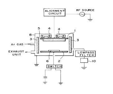
Fig. 1 is a partial schematic cross-sectional
view of a plasma processing apparatus of the present
invention, adapted for use as a sputtering apparatus.
There are shown a first electrode 1 which is
connected through a matching circuit to a high frequency
(RF) power source serving as a plasma generating power
source and which can support a marget material 5; a
second electrode 2 capable of supporting a substrate
and being maintained at a ground potential or a floating
potential by a switch; a third electrode 3 enclosing
the space between the first electrode 1 and the second
electrode 2; magnets 4 for inducing magnetron discharge
on the target 5; a target material 5; a substrate 6;
a vacuum chamber 8; and a power source 10 for controlling
the potential of the third electrode 3 through a low-
pass filter. The third electrode can be composed of
a non-insulating material such as stainless steel,
Cu, A1, Ta, Mo, Nb, Ti or Si. Said third electrode
can be fixed to the vacuum chamber by an insulating
member composed for example of alumina, ceramics or
glass.
The film formation in the above-explained
Zo ~a4 ~o
_ 11 _ _ _
1 apparatus can be conducted, for example, in the
following manner.
The substrate 6 is mounted on the second
electrode 2, then the vacuum chamber 8 is evacuated
to a predetermined pressure by a vacuum unit, and the
third electrode 3 is maintained at a predetermined
potential. Then inert gas such as argon is introduced
into the vacuum chamber 8, with a predetermined pressure.
An RF potential is applied to the first electrode 1
to induce discharge, thus generating plasma and effecting
film formation.
The potential of the third electrode is suitably
selected according to the film forming conditions to
be employed and the effects to be attained by the third
electrode.
For example, as will be shown in the following
examples, the effects shown in Figs. 2A to 2C can be
attained by suitable selection of the potential of
the third electrode.
The structure of the third electrode is not
limited as long as it can therein accommodate the first
electrode 1 and the second electrode 2.
For example, it may have a cylindrical structure,
as shown in Fig. 9, eventually with an aperture 9 for
loading and unloading of the substrate.
In the apparatus shown in Fig. 1, the arrangement
of magnets for application of magnetic field around
20 484 70
- 12 -
1 the target may be suitably modified, for example outside
a vacuum chamber 1308 as shown in Fig. 13. Also the
potential of the substrate 6 may be controlled for
example by a DC power source through a low-pass filter
or by an RF power source through a matching circuit
to be explained later.
Fig. 3 illustrates another embodiment of the
plasma processing apparatus of the present invention,
which can also be utilized as a sputtering apparatus.
There are shown a first electrode 301 which
is connected to a plasma generating RF power source
through a matching circuit and which can support a
target material 305; a second electrode 302 capable
of supporting a substrate and maintained at the ground
potential; a third electrode 303 serving also as a
vacuum chamber; magnets 304 for inducing magnetron
discharge on the substrate; a target material 305;
a substrate 306; and a power source 310 for potential
control of the third electrode 303 through a low-pass
filter.
The film formation with the above-explained
apparatus can be conducted for example in the following
manner.
The substrate 306 is mounted on the second
electrode 302, then the vacuum chamber consisting of
the third electrode 303 is evacuated to a predetermined
pressure by a vacuum unit, and said third electrode
20 484 70
_ 13 _ i
1 303 is maintained at a predetermined potential. Then
..inert gas such as argon is introduced with a predeter-
mined pressure into said vacuum chamber, and an RF
potential is applied to the first electrode 301 to
induce discharge, thereby effecting film formation.
As in the foregoing embodiments, the potential
of the third electrode is suitably selected according
to the film forming conditions and the effects to be
attained.
Fig. 5 shows another embodiment of the plasma
processing apparatus of the present invention, in which
the third electrode is divided into plural portions
of which potentials can be independently controlled.
There are provided a first electrode 501 con-
nected to a plasma generating RF power source through
a matching circuit and capable of supporting a target
material 505; a second electrode 502 capable of
supporting a substrate 506 and being maintained at
the ground potential or at a floating potential by
a switch; a third electrode 503 of the substrate side
positioned in the vicinity of the substrate; a third
electrode 513 of the target side positioned in the
vicinity of the target; magnets 504 for inducing
magnetron discharge on the target 505; a target material
505; a substrate 506; a vacuum chamber 508; a power
source 510 for controlling the potential of the third
electrode of the substrate side through a low-pass
20 ~s4 ~o
- 14 - _
1 filter; and a power source 511 for controlling the
potential of the third electrode of the target side
through a low-pass filter.
Film formation in the above-explained apparatus
is conducted in the following manner.
The substrate 506 is mounted on the second
electrode 502, then the vacuum chamber 508 is evacuated
to a predetermined pressure by a vacuum unit, and the
third electrode 503 of the substrate side and that
513 of the target side are regulated at predetermined
potentials. Then an RF potential is applied to the
first electrode 501 to induce discharge, thereby effect-
ing film formation.
The manner of division of the third electrode
is not limited to the illustrated one but may be
conducted in various ways according to the necessity.
More specifically, in the illustrated example,
the cylindrical third electrode is divided along the
circumference thereof (horizontally in the illustration)
into two portions, but it is also possible to effect
the division into three or more portions, or in the
circumferential and/or axial (vertical) direction.
The potentials of thus divided third electrodes
are suitably selected according to the film forming
conditions and the effects to be attained by said third
electrodes.
The above-explained divided structure of the
- 15 - 20 484 70
1 third electrode allows to improve the controllability
..on the spatial distribution of the plasma potential.
The entry of contaminants from the vacuum
chamber 508 into the film can be almost completely
prevented as long as the gap between the third electrode
503 of the substrate side and that 513 of the target
side does not exceed several millimeters. Also the
entry of such contaminants can be more securely
prevented by filling said gap of the third electrodes
503, 513 with an insulating material.
Fig. 7 shows another embodiment of the plasma
processing apparatus of the present invention, which
can be utilized as a sputtering apparatus.
There are provided a first electrode 701
connected to a plasma generating RF power source through
a matching circuit and capable of supporting a target
material 705; a second electrode 702 capable of
supporting a substrate 706 and connected to an RF
power source through a matching circuit; a third
electrode 703 enclosing a space between the first
electrode 701 and the second electrode 702; magnets 704
for inducing magnetron discharge on the target material
705; a target material 705; a substrate 706; a vacuum
chamber 708; and a power source 710 for potential
control of the third electrode through a low-pass
filter.
Film formation in the above-explained apparatus
a
A
- 16 -
20 X84 70
1 is conducted in the following manner.
The substrate 706 is mounted on the second
electrode 702, then the vacuum chamber 708 is evacuated
to a predetermined pressure by a vacuum unit, and the
potentials of the third electrode 703 and of the second
electrode 702 are respectively regulated at predetermined
values. Then RF potentials are supplied to the first
electrode 701 and the second electrode 702 to induce
discharge, thereby effecting film formation.
As in the foregoing embodiments, the potential
of the third electrode is suitably selected according
to the film forming conditions and the effects to be
attained by the third electrode.
In the above-explained apparatus, the potential
to be supplied to the second electrode may be a DC
potential if the substrate 706 placed on the .second
electrode 702 is conductive.
The cylindrical third electrode employed in
the foregoing embodiments may also be provided with an
aperture 9, as shown in Fig. 9, with a frame member
that can be utilized as a guide in the transportation
of the substrate, or, as shown in Fig. 11, with a door
to improve the intercepting property of the third
electrode during the film formation.
Furthermore, as shown in Fig. 14, it is possible
to support the third electrode movably in the vertical
direction by means of an insulating member 18 and a
17
1 shaft 20 connected to bellows 19, thereby lifting said
-third electrode at the loading and unloading of the
substrate and to place said electrode at the illustrated
position at the film formation.
The present invention has been explained by
various embodiments thereof, but the present invention
is not limited to such embodiments and is subject to
various modifications within the scope and spirit of
the appended claims.
Also the plasma processing apparatus of the
present invention is applicable not only to the film
formation by sputtering but also to plasma CVD or sputter
etching.
Example 1
Silicon film formation was conducted with the
apparatus shown in Fig. l, under following conditions:
RF power supplied to the first electrode: 100 MHz,
100 W,
Potential of the second electrode: floating potential
or ground potential (0 V),
Potential of the third electrode: -40 - 60 V (40 V),
Introduced gas: Ar (1000 , flow rate: 100 sccm,
Vacuum chamber pressure at film formation: 5 mTorr,
Lowest pressure reached in the vacuum chamber:
1.2 x 10⁻⁹ Torr
Substrate temperature: 350°C
Target material: Si
18 20 X84 70
1 Substrate: Si wafer.
The measured control range of the incident ion
energy when the substrate was maintained at the ground
potential is shown in Fig. 2A.
The incident ion energy was measured with a
Faraday cup of reflective electric field type.
Also Fig. 2C shows the result of measurement
by SIMS (secondary ion) mass spectroscopy, on the
concentration of Fe, which is the principal component
of the vacuum chamber and the third electrode,
incorporated into the Si film formed on the substrate.
Also Fig. 2B shows the control range of the
incident ion energy when the substrate was maintained
at the floating potential.
Similar results could be obtained also by
controlling the substrate potential with a DC power
source through a low-pass filter or with an RF power
source through a matching circuit.
Reference Example 1
Silicon film formation was conducted with the
apparatus shown in Fig. 12, under the same conditions
as those in the example 1, and measurement were
conducted as in the example 1. The results are shown
in Figs. 2A to 2C.
Comparison of the results of the example 1
and the reference example 1 reveals following advantages
of the apparatus of the example 1.
_ 19 2048470
1 As shown in Fig. 2A, when the substrate was
maintained at the ground potential, the control range
of the incident ion energy in the example 1 was 4 -
60 eV (third electrode potential -40 - 40 V), thus
being extended in the low energy side, in comparison
with that in the reference example 1 of 20 - 60 eV
(third electrode potential -40 - 40 V). Also when
the substrate was maintained at the floating potential,
as shown in Fig. 2B, the control range of the incident
ion energy in the example 1 was 3.5 - 23.5 eV (third
electrode potential -40 - 60 V), thus again extended
in the low energy side, in comparison with 16 - 24
eV (third electrode potential -40 - 60 V). Furthermore,
as shown in Fig. 2C, the Fe concentraiton in the Si
film formed with the substrate maintained at the ground
potential under same discharge conditions was about
10 times smaller for example in the comparison of minimum
values.
The above-explained facts reveal that the use
of a third electrode enclosing the space between the
first and second electrodes and the control of potential
of said third electrode provide the effects of extending
the control range of the incident ion energy to the
substrate, in comparison with the potential control
of the third electrode 33 positioned in the vicinity
of the target in the conventional apparatus (reference
example 1), and of reducing the contamination of the
20 484 70
- 20 -
1 film from the vacuum chamber 8 and the third electrode
..3 (or 33).
Example 2
Film formation was conducted with the apparatus
shown in Fig. 3, with following conditions:
RF power to the first electrode: 100 MHz, 100 W,
Potential of the second electrode: ground potential
(0 V) ,
Potential of the third electrode: -40 - 60 V
Introduced gas: Ar (1000 , flow rate: 100 sccm,
Vacuum chamber pressure at film formation: 5 mTorr,
Minimum pressure reached in vacuum chamber: 1.2 x
109 Torr,
Substrate temperature: 350°C
Target material: Si,
Substrate: Si wafer.
The control range of the incident ion energy
at the film formation was measured in the same manner
as in the example 1, with results shown in Fig. 4A.
In the above-mentioned apparatus, the energy of the
ions incident to the substrate could be varied in a
range of 3 - 84 eV (third electrode potential: -40 -
60 V) .
Fig. 4B shows the result of measurement by
SIMS on the Fe concentration present in the formed
Si film and resulting from the third electrode 303.
The results indicate that the Fe concentration can
- 21 -
2~4-8~-7~
1 be maintained below the detection limit (below 1 x
..015 atom/cm3, by maintaining the third electrode
potential within a range of -15 to -5 V or at 5 V.
Example 3
Film formation was conducted with the apparatus
shown in Fig. 5 and under following conditions:
RF power to the first electrode: 100 MHz, 100 W,
Potential of the second electrode: floating potential
or ground potential (0 V),
potential of the third electrode at the substrate
side: -5 V,
Potential of the third electrode at the target
side: -40 - 60 V,
Introduced gas: Ar (1000 , flow rate: 100 sccm,
Vacuum chamber pressure at film formation: 5 mTorr,
Minimum pressure reached in vacuum chamber: 1.2 x
10-9 Torr,
Substrate temperature: 350°C,
Target material: Si,
Substrate: Si wafer.
The control range of the incident ion energy
in the film formation under the above-mentioned condi-
tions with the second electrode maintained at the ground
potential (0 V), measured as in the example 1, was
3 - 75 eV (potential of the third electrode at the
target side: -40 - -60 V), as shown in Fig. 6A.
The Si film forming speed varied in a range
- 22 - ~ 0 _.
0
1 of 2 - 3 A/sec. according to the potential of the third
electrode at the target side, as shown in Fig. 6B.
Also in the film formation with the substrate
maintained at the floating potential and under the
above-mentioned conditions, the control range of the
incident ion energy and the Si film forming speed
respectively varied in a range of 3 - 22 eV as shown
0
in Fig. 6A and in a range of 1.8 - 3.8 A/sec. as shown
in Fig. 6B, according to the variation in the potential
of the third electrode at the target side.
These facts indicate that the divided structure
of the third electrode in the target side and the
substrate side in the apparatus of this example can
increase the film forming speed without change in the
energy of ions incident to the substrate 506, in the
potential control of the third electrode 513 at the
target side, in comparison with the apparatus shown
in Fig. 1 employing an undivided third electrode, thereby
further improving the productivity while maintaining
the high quality of the film.
Example 4
Film formation was conducted with the apparatus
shown in Fig. 7, under the following conditions:
RF power to the first electrode: 100 MHz, 100 W,
Power to the second electrode: 177 MHz, 0 - 100 W,
Potential of the third electrode: -5 V,
Introduced gas: Ar (100$), flow rate: 100 sccm,
- 23 - 20 484 70
1 Vacuum chamber pressure at film formation: 5 mTorr,
Minimum pressure reached in vacuum chamber: 1.2 x
10-9 Torr,
Substrate temperature: 350°C,
Target material: Si,
Substrate: Si wafer.
Under the above-mentioned conditions, there was
obtained a relationship shown in Fig. 8A between the
substrate potential and the power supplied to the second
electrode. Stated differently, in the apparatus of
the present example, the substrate potential could
be controlled within a range of +4 to -27 V by varying
the power to the second electrode within a range of
0 - 100 W.
Also there was obtained a relationship shown
in Fig. 8B between the incident ion energy and the
power supplied to the second electrode at the film
formation. Stated differently, in the present apparatus,
the incident ion energy could be controlled within
a range of 3 - 34 eV by varying the power to the second
electrode within a range of 0 - 100 W.
Also the change in crystallinity of the Si
0
film (thickness: 1000 A) under different powers to
the second electrode was investigated by electron beam
diffraction, as shown in Table 1:
- 24 -
1 Table 1
Power to second
electrode (W) 0 10 20 30 40 50 60 80 100
Electron beam
diffracted image + + ++ ++ + + + - -
wherein ++ indicates a Kikuchi's line; + indicates
a streak; and - indicates a hallow.
As will be apparent from Tab. 1, it is possible
to control the crystal structure of the film deposited
on the substrate 706 by controlling the potential of
the third electrode 703 enclosing the space between
the first electrode 701 and the second electrode 702,
applying an RF potential to the second electrode 702
and controlling the power supplied from the RF power
source.
For example the electron beam diffracted image
shows Kikuchi's line with a power of 20 - 30 W to the
second electrode, so that a Si film can be epitaxially
grown on the Si wafer by film formation under the above-
mentioned condition.
Also Fig. 8C indicates the concentration,
measured by SIMS, of Fe which is the principal component
of the vacuum chamber 708 and the third electrode 703
and which is incorporated in the Si film formed with
the power of 0 - 100 W supplied to the second electrode.
As shown in Fig. 8C, the Fe concentration in the obtained
film was below the detection limit.
Also similar results were obtained by employing
- 25 -
1 a conductive substrate 706 and effecting the potential
supply to the second electrode with a DC power source.
10
20