Note : Les descriptions sont présentées dans la langue officielle dans laquelle elles ont été soumises.
2049448
VERTICAL CAVITY TYPE VERTICAL TO SURFACE
TRANSMISSION ELECTROPHOTONIC DEVICE
FIELD OF THE INVENTION
This invention relates to a vertical cavity type
vertical to surface transmission electrophotonic device
(defined "VC-VSTEP" hereinafter), and more particularly
to, a VC-VSTEP applicable to a high density parallel
light transmission system, an optical information
processing system, etc.
BACKGROUND OF THE INVENTION
A vertical to surface transmission
electrophotonic device (defined "VSTEP" hereinafter) in
which light is emitted from and received in the device
in the vertical direction to a semiconductor substrate
is a key device which is indispensable for data
transmission among computers and for optical computing
therein.
A light emitting device type vertical to surface
transmission electrophotonic device (defined "LED-
VSTEP" hereinafter) is one of conventional VSTEPs. In
the LED-VSTEP, light emission of sponteneous emission
mode occurs in the vertical direction to a
semiconductor substrate.
A laser diode type VSTEP of induced emission
mode (defined "LD-VSTEP" hereinafter) is also
2049448
developed, and is the other one of the conventional
VSTEPs. This LD-VSTEP comprises a cavity formed in the
horizontal direction to a semiconductor substrate, and
may comprises a reflecting mirror provided to have an
angle of 45 relative to an active layer, so that light
is emitted in the vertical direction to the substrate,
as described on pages 329 to 331 of "Appl. Phys. Lett.
Vol. 54, No. 4 January 1989.
However, the conventional LED-VSTEP has
disadvantages in that electrophotonic converting
efficiency is not high, frequency response speed is not
fast, and output light directivity is not good,
respectively, as expected, because the light emission
is of the spontaneous emission mode.
In addition, the conventional LD-VSTEP has
disadvantages in that the size of the device is
difficult to be small, because a cavity is formed in
the horizontal direction to the semiconductor
substrate, and light absorption efficiency is low at
the same wavelength as an oscillation wavelength,
because an absorption layer and an active layer are
provided separately from each other. There is a
further disadvantage in the conventional LD-VSTEP in
that photosensitivity is lowered in case where devices
are connected in cascade.
SUMMARY OF THE INVENTION
204q448
71885-22
Accordingly, it is an object of the invention to provide
a VC-VSTEP from which light emission of induced emission mode
occurs in the vertical direction to a semiconductor substrate
without the necessity of a 45 reflecting mirror.
It is a further object of the invention to provide a VC-
VSTEP having predetermined properties in electrophotonic
converting efficiency, frequency response speed, and output light
directivity.
It is a still further object of the invention to provide
a VC-VSTEP which can be small in size.
It is a yet still further object of the invention to
provide a VC-VSTEP having predetermined light absorption
efficiency and photosensitivity.
According to one aspect of the present invention, a VC-
VSTEP, comprises~ a pnpn structure; a quantum well structure
provided in said pnpn structure and functioning as a light
absorption layer and an active layer; first and second optical
guide structures provided above and below said quantum well
structure and being part of said pnpn structure; and first and
second multi-layered mirror structures provided above said first
optical guide structure and below said second optical guide
structure and being part of said pnpn structure; wherein a total
optical thickness of said quantum well structure and said first
and second optical guide structures is set to be n times an
oscillation wavelength, where n is an integer, and said first and
second multi-layered mirror structures having asymmetrical
reflectivities to provide a vertical cavity, whereby a light
204~44~
71885-22
absorption factor is increased therein.
According to another aspect, the present invention
provides a vertical cavity type vertical to surface transmission
electrophotonic device, comprising: a semiconductor substrate of a
first conductivity type; a lower DBR mirror provided on a first
surface of said semiconductor substrate, and including a plurality
of first conductivity type layers having first and second
refractive indices alternately provided; a lower optical guide
layer provided on a first surface of said lower DBR mirror, and
including a second conductivity type layer and an intrinsic type
layer; an active layer provided on a first surface of said lower
optical guide layer, and including a plurality of quantum well
layers; an upper optical guide layer provided on a first surface
of said active layer, and including an intrinsic type layer and a
first conductivity type layer; an upper DBR mirror provided on a
first surface of said upper optical guide layer, and including a
plurality of second conductivity type layers having said first and
second refractive indices alternately provided; a first electrode
provided on a first surface of said upper DBR mirror; and a second
electrode provided on a second surface of said semiconductor
substrate, and having an aperture for input and output of light.
BRIEF DESCRIPTION OF THE DRAWINGS
The invention will be explained in more detail in
conjunction with appended drawings, wherein:
Fig. 1 is a schematic cross-sectional view showing a
conventional LED-VSTEP;
2049448
71885-22
Fig. 2 is a schematic cross-sectional view showing a
conventional LD-VSTEP;
Fig. 3 is a schematic cross-sectional view showing a VC-
VSTEP in a preferred embodiment according to the invention;
Fig. 4 is an explanatory diagram explaining the increase
of light absorption in the VC-VSTEP;
Fig. S is a graph explaining a property of light output
relative to current and current relative to voltage in the VC-
VSTEP;
Fig. 6 is a graph explaining slope efficiency and
oscillation threshold gain and current density relative to the
number of lower DBR mirror layers; and
4a
5 2049448
Fig. 7 is a graph explaining light absorption
factor and light switching energy relative to the
number of lower DBR mirror layers.
DESCRIPTION OF THE PREFERRED EMBODIMENT
5Before describing a VC-VSTEP according to the
invention, the aforementioned conventional LED-VSTEP
and LD-VSTEP will be explained in Figs. 1 and 2.
Fig. 1 shows the conventional LED-VSTEP which
comprises a semiconductor substrate 11 of Si-GaAs, a
10buffer layer 12 of n-GaAs, a cathode layer 13 of n-
AlGaAs, a charge sheet layer 14 of p-GaAs, a gate layer
15 of n-GaAs, an anode layer 16 of p-AlGaAs, and a cap
layer 17 of p-GaAs. The conventional LED-VSTEP further
comprises an anode electrode 18 provided on the cap
15layer 27, and a cathode electrode 19 provided on the
buffer layer 12.
In operation, a predetermined bias voltage is
applied across the anode and cathode electrodes 18 and
19, so that output light of spontaneous emission mode
20is emitted in the vertical direction to the substrate
11 from an aperture of the anode electrode 18, as shown
by an arrow.
Fig. 2 shows the conventional LD-VSTEP which
comprises a semiconductor substrate 21 of n-GaAs, a
25buffer layer 22 of n-GaAs, a cathode layer 23 of n-
Alo 4Ga0 6As, a p-gate layer 24 of p+-Alo 25Ga0 75As,
6 204q448
undoped layers 25 and 27 of i-Al0.25Ga0.75As, an act v
l ayer 26 of i-GaAs, an n-gate l ayer 28 of n-
Alo 25Ga0 25As, an anode layer of p-Alo 4Ga0 6As, a cap
layer 30 of p+-GaAs, and an insulation film layer 31 of
SiO2. The LD-VSTEP further comprises a p-electrode 32
of Au/Cr which is in partly contact with the cap layer
30, and an n-electrode 33 of AuGaNi which is provided
on the back surface of the substrate 21.
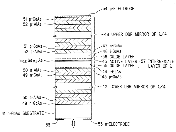
Next, a VC-VSTEP of a preferred embodiment
according to the invention will be explained in Fig. 3.
On a semiconductor substrate 41 of n-GaAs, a
lower DBR mirror 42 having a doping concentration of 5
x 1 o1 7cm-3, a p-GaAs layer 43 having a doping
concentration of 1 x 1019cm 3 and a thickness of 50 A,
an undoped Alo 25Ga0 75As having a thickness of less
than 1500 A, an undoped InO 2Ga0 8As layer 45 for an
active layer including three quantum well layers each
having a thickness of 100 A (in detail, each quantum
layer including a 100 A well layer of InO 2Ga0 8As and
a 100 A barrier layer of Al0.25Ga0.75As), a p
Alo 25Ga0 75As layer 46 having a thickness of less than
500 A, an n-GaAs layer 47 having a doping concentration
of 3 x 1 o1 7cm 3 and a thickness of less than 1000 A,
and an upper DBR mirror 48 having a doping
concentration of 5 x 1018cm 3 are successively grown by
the molecular beam epitaxial method. The lower DBR
mirror 42 is composed of 14.5 pairs of n-GaAs layers 49
204q448
each having a thickness of approximately 672 A and n-
AlAs layers 10 each having a thickness of approximately
804 A which are grown alternately, and the upper DBR
mirror 48 is composed of 15 pairs of p-GaAs layers 51
each having a thickness of approximately 672 A and p-
AlAs layers 52 each having a thickness of approximately
804 A which are grown alternately. In addition, there
are provided an n-electrode 53 on the back surface of
the substrate 41, and a p-electrode 54 on the upper DBR
mirror 48.
In the VC-VSTEP, the p-GaAs layer 43 and the i-
GaAs layer 44, and the i-GaAs layer 46 and the n-GaAs
layer 47 provide optical guide layers 55 and 56,
respectively, and the optical guide layers 55 and 56
and the active layer 45 provide an intermediate layer
47. A thickness of the intermediate layer 47 is set in
this preferred embodiment to be n times of a wavelength
in a medium of laser osci l lation, where n is an
integer. Here, the wavelength is approximately 0.3
l m, assuming that a cavity wavelength is 9500 A.
In principle, a VSTEP is a light emitting and
receiving device having functions of threshold
processing and memory by including a pnpn structure.
In the VC-VSTEP, the quantum well layers 45 function as
an active layer at the time of ON, and an absorption
layer at the time of OFF, and it is expected that the
effect of absorption is increased, and a absorption
8 2049448
wavelength band and an oscillation wavelength become
equal, respectively, by a vertical cavity which is
provided to be asymmmetrical therein.
As described above, the active layer 45 which is
for the absorption layer at the time of OFF has a
thickness of only 300 A. Ordinarily, a light
absorption factor which is obtained in an absorption
layer of such a thin thickness is no more than
approximately 3%, even if an absorption coefficient is
estimated to be 10000 cm~1 which is considered to be
the largest value. In the invention, however, the
light absorption factor becomes much greater in
accordance with the effect of multi-reflection caused
by the multi-reflection layers of the lower and upper
DBR mirrors 42 and 48 (cavity effect).
In the invention, a thickness of the
intermediate layer 57 including the active layer 45 is
set to be n times of a resonant wavelength in the
medium, so that lights reflected in the lower and upper
DBR mirrors 42 and 48 are out of phase. Accordingly,
light having a wavelength which just resonates with the
cavity are reflected with the largest intensity by the
lower and upper DBR mirrors 42 and 48, so that the
reflected lights are cancelled due to the "out of
phase". In the invention, the asymmetrical cavity
structure is optimized to provide the lower and upper
DBR mirrors 42 and 48 with reflection factors which are
9 204~448
based on the consideration of an absorption coefficient
of the active layer 45, so that reflection and
transmission of light can be almost negligible, and the
absorption factor can be large.
Fig. 4 shows a light intensity distribution ID
in the intermediate layer 57 and the lower and upper
DBR mirrors 42 and 48, and a refractive index
distribution ND therein. As clearly shown therein, the
refractive index distribution ND is defined by
refractive indices N1 (=2.9) of the AlAs layers and N2
(=3.6) of the GaAs layers for the lower and upper DBR
mirrors 42 and 48, and a refractive index N3 for the
intermediate layer 47 which is higher than the
refractive index N1 and lower than the refractive index
N2, in addition to a refractive index No of air shown
to be "1" therein. For this refractive index
distribution ND, an input light is transmitted through
the lower DBR mirror 42 and the intermediate layer 57,
and reflected on an interface between the intermediate
layer 47 and the upper DBR mirror 48 and an interface
between the intermediate layer 47 and the lower DBR
mirror 42, repeatedly, as shown by an arrow. In this
light reflection, a phase difference of ~ occurs
between the two interfaces. As described before, the
number of the lower and upper DBR mirrors 42 and 48 is
optimized, so that the increase of light intensity
occurs in the intermediate layer 57 to provide an
10 2049448
absorption factor which is as high as 99.92%, despite
the structure in which the absorption layer (the active
layer 45) is as thin as 300 A. Thus, the light
intensity distribution ID is obtained as shown therein.
Ordinarily, a wavelength of laser oscillation is
positioned on a side of energy which is lower than an
absorption band, so that a problem in which an
absorption coefficient of the absorption layer (an
active layer) becomes low at the oscillation wavelength
occurs. In the invention, however, laser light is
effectively absorbed, because a reverse bias voltage is
applied to the absorption layer (the active layer 45)
at the time of OFF to result in the confinement of
quantum, so that an absorption band is shifted in the
direction of long wavelength by the optical Stark
effect.
In operation, when a bias voltage is applied
across the n- and p-electrodes 53 and 54, the input and
output of light is carried out through the n-GaAs
substrate 41.
Fig. 5 shows a light output relative to a
current flowing through the VC-VSTEP (Fig. 3) which has
a size of 20 x 20 ~m2 and is turned on at a room
temperature by a pulse having a width of 20 ns, a
repetition rate of 50 kHz and a duty ratio of 1/1000 to
be applied thereto, and a current relative to a voltage
in the form of the pulse applied to the VC-VSTEP under
11 2049448
the same state. As shown therein, the maximum light
output is 127 mW. Otherwise, a switching voltage for
turning the VC-VSTEP on is 6 V, and a holding voltage
for holding the ON state of the VC-VSTEP is 2 V. These
voltage values are the same as those of a VC-VSTEP to
be designed.
Fig. 6 shows a slope efficiency and oscillation
threshold gain and current density relative to the
number of layers in the lower DBR mirror 42 of the VC-
VSTEP, wherein the slope efficiency and the oscillation
threshold gain and current density are measured in the
VC-VSTEP having the upper DBR mirror of 15 pairs and
the p-electrode of Au as shown by points P1 to P4, when
the number is 14.5 pairs (the preferred embodiment) and
24.5 pairs, respectively. As clearly shown therein,
the slope efficiency is improved from 0.06 mW/mA at
24.5 pairs to 0.32 mW/mA at 14.5 pairs by approximately
more than 5 times, as shown by the points P1 and P2.
Similarly, the oscillation threshold gain and current
density are also improved by approximately 3 times, as
shown by the points P3 and P4. At the same time, a
solid curve and a dotted curve which are obtained by
calculation are also shown to indicate the improvement
of the oscillation threshold gain and current density
and the slope efficiency. For the oscillation
threshold gain and current density, the experiment and
calculation results are coincided. For the slope
12 204q448
efficiency, however, the experiment result indicated by
the point P2 is lower than the calculation result
indicated by the dotted curve, because a reflection
factor of the p-elecrode of Au-Zn is lower than that of
the p-electrode of Au, and a dispersion loss is not
considered in the lower and upper DBR mirrors.
Fig. 7 shows an absorption factor and an optical
switching energy relative to the number of layers in
the lower DBR mirror 42 of the same VC-VSTEP as that
used in Fig. 6, in which an absorption coefficient of
the active layer 45 is 3000 cm~1, wherein points P1 and
P2 indicates experiment results, while a solid curve
indicates a calculation result. The optical switching
energy is improved from 14 pJ at 25 pairs to 0.5 pJ at
15 pairs by approximately 30 times, when the VC-VSTEP
is converted to be a VC-VSTEP having a size of 10 x 10
~m2 and a switching speed of 10 ns. This improved
value is the same as a value to be designed, and it is
considered that this result is based on the increase of
light absorption by the asymmetrical cavity.
Although the invention has been described with
respect to specific embodiment for complete and clear
disclosure, the appended claims are not to be thus
limited but are to be construed as embodying all
modification and alternative constructions that may
occur to one skilled in the art which fairly fall
within the basic teaching herein set forth.