Note : Les descriptions sont présentées dans la langue officielle dans laquelle elles ont été soumises.
2049544
LOGARITHMIC AMPLIFIER/DETECTOR DELAY COMPENSATION
FIELD OF INVENTION
The present invention relates to logarithmic
amplifiers for use in pulse receiver systems, and more
particularly to a system for compensating for time delays in
radio signal amplifier/detector chains.
BACKGROUND OF THE INVENTION
The strength or amplitude of a received radio
signal is typically measured by a device commonly known as a
detector. In its simplest form, a detector may be a diode
rectifier which converts an A.C. radio signal to a D.C.
voltage proportional to the amplitude of the radio signal.
In practice, the detector has a minimum signal level below
which it will not produce a usable output. Accordingly,
amplifiers are employed to generate a detectable signal.
Another constraint is that the maximum detectable signal is
limited both by the detector's breakdown voltage and an
individual amplifier's saturation voltage. The detector's
dynamic signal range is defined by these minimum and maximum
signal levels.
To overcome limitations in the detector's dynamic
range, logarithmic amplifiers are used. Logarithmic radio
frequency (RF) amplifiers typically employ a chain of RF
amplifiers of similar gain for cascade amplification of the
input signal. Each amplifier provides an output that is a
substantially linear function of the input signal until the
input signal reaches a sufficient amplitude to saturate that
amplifier. When this amplitude level is reached, the output
of the amplifier remains constant at that limiting amplitude
.. despite increases in the input signal level. Typically, if
the signal level is very small, only by the final amplifier
stage would the signal level have reached a detectable
level. Conversely, if the signal level is large, the
2049544
- 2 -
amplifiers will saturate in reverse order beginning with the
last amplifier.
A significant problem with using a logarithmic
amplifier chain having a large number of stages and a high
total gain is the amplification of noise signals over a wide
frequency range: In the absence of an input signal,
internal amplifier noise could drive the later amplifier
stages into saturation. In order to prevent premature
saturation caused by wideband noise and to allow higher
overall gain, the bandwidth must be restricted. One or more
filters can be interposed between amplifier stages to limit
the bandwidth so that only frequencies at or near the input
signal frequency are amplified. In addition, to avoid
instability caused by feedback between the input and output
of a long amplifier chain, one or more frequency
conversions may be required in the middle of such a chain in
order to split the total desired amplification over
different intermediate frequencies. The use of heterodyne
mixers to effect frequency conversion may also involve
bandwidth restricting filters to suppress unwanted frequency
outputs or other spurious responses.
Unfortunately, the restriction of bandwidth
necessarily introduces a time delay in the signal. For
example, inserting a bandwidth limiting filter between first
and second amplifier stages delays the output signal from _
the first stage to the second stage by a certain time
period. Bandwidth restrictions in a logarithmic amplifier
chain cause successive time delays in the responses of
successive detector stages. Consequently, the sum of the
detected outputs no longer represents the logarithm of the
instantaneous signal amplitude.
2049544
- 3 -
Accordingly, it is desirable to provide a
logarithmic amplifier/detector that overcomes the
limitations of prior logarithmic amplifiers. Specifically,
it is desirable to restrict the bandwidth of amplified
signals and at the same time compensate for the resulting
time delay in order to reduce transient distortion.
SiJMMARY OF THE INVENTION
The present invention resides in an
amplifier/detector chain designed to logarithmically amplify
an input signal as well as compensate for delays generated
by necessary bandwidth restrictions. A plurality of
amplifiers are connected in series and grouped in amplifier
stages with each stage having at least one amplifier. In
between each amplifier stage is a filter which restricts the
bandwidth of signals which it will amplify to frequencies in
the desired input signal range. When an amplifier stage
includes more than one amplifier, a local summer sums the
outputs detected by detectors associated with each amplifier
in a particular stage. When an amplifier stage includes
only a single amplifier and associated detector, the local
sum signal for the stage is simply the detector output. No
local summer is required. Because of the time delay
introduced by each interposed filter, each local sum is
input to a corresponding compensating device which
compensates for the associated time delay. Each
compensating device stores its corresponding local sum until
the local sum from the final stage is ready to be output.
When all of the local summer outputs have been time-aligned
or brought in phase, the local sums are connected from their
corresponding compensating devices to a central summer
stage. The output of the central summer represents the
2049544
- 4 -
instantaneous output of the logarithmically amplified input
signal.
BRIEF DESCRIPTION OF THE DRAWINGS
These and other features and advantages of the
invention will be readily apparent to one of ordinary skill
in the art from the following written description, read in
conjunction with the drawings, in which:
Figure 1 is a general schematic view of a
logarithmic amplifier/detector chains
Figure 2 is a general schematic view of a system
for implementing the present invention
Figure 3 is a more detailed schematic view of a
system for implementing the present invention; and
Figure 4 is a timing diagram which shows various
wave- forms useful in understanding the present invention.
DETAILED DESCRIPTION OF THE PREFERRED EMBODIMENTS
To further facilitate an understanding of the
invention, a conventional logarithmic amplifier is described
with reference to Figure 1. An input radio signal Si is
received by a first amplifier 1a which amplifies the input
signal by a suitable gain factor. The output of the
amplifier la is detected by a detector 2a and received as an
input signal by the next amplifier lb. Each detector output
is connected to a central summing device 3 which generates
an amplified output signal So.
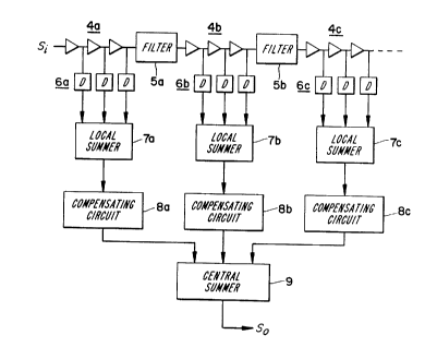
Figure 2 shows a general schematic of a system for
implementing the present invention. It will be
appreciated, however, that specific applications of the
invention are not limited to radio receiver detectors.
Rather, the present invention is applicable to any situation
X049544
- 5 -
where it is desirable to compensate for propagation delays
in an amplifier chain.
An input signal Si is fed to a first stage of
amplifiers 4a. Each stage of amplifiers, represented in the
drawings by three individual amplifiers, has at least one
amplifier but may contain more than one amplifier. In the
preferred embodiment, each stage of amplifiers contains
plural arplifiers. The output of each amplifier in stage 4a
is connected to a respective detector 6a. Each detector 6a
is typically a half wave rectifier. At this point it should
be made clear that when an amplifier stage includes more
than one amplifier, a local summer 7a sums the output
detected by each detector 6a associated with each amplifier.
When an amplifier stage includes only a single amplifier and
associated detector, the local sum signal for that stage is
simply the detector output. No local summer is required.
The output of the local summer ~a is input to a
compensating circuit 8a. The output of compensating circuit
8a becomes one of several inputs to a central summing device
9. The signal output So of the central summing device 9
represents the output of the logarithmic amplifier chain.
Interposed between each local amplifier stage is a
filter. For example, a filter 5a is interposed between
local amplifier stages 4a and 4b. Likewise, a filter 5b is
interposed between local amplifier stages 4b and 4c. The
system in the Figure 2 shows three individual amplifier,
detector, summing, and compensating stages which then
connect to a central summing device. Of course, additional
stages could be used in the present invention.
As discussed previously, each filter interposed
between the local amplifier stages intraduces a
corresponding delay. In this example, it is assumed that
20495~~
- 6 -
the only significant delays are caused by the filters and
not the amplifiers themselves. Accordingly, the three
locally summed signals S1, S2, S3 are delayed relatively by
the time delay period T1 arising in filter F1, which delays
signals S2 and S3, and time delay period T2 in filter F2
which further delays signal S3. Assuming the time delay
periods are substantially equivalent, the local sum S1 is
out of phase by two time delay periods, and the local sum S2
is out of phase by a single time delay period. Since
negative delays are scientifically impossible to accomplish,
the local sum S2 must be delayed by time delay period T2 and
local sum S1 must be delayed by two time delay periods T1 +
T2 to time-align them with local sum S3.
Consequently, if there are "n" amplifier stages,
the output of the i-th amplifier stage will be delayed by
(n-i) time periods T(i) + T(i+1) + ... + T(n-1), where
"T(i)" is the filter delay between the i-th and (i+1) - th
amplifier stages. For example, if n=3 and i=1, the local
sum S1 will be delayed by (3-1)=2 time periods.
Figure 3 is a more detailed schematic diagram of a
circuit incorporating the principles of the invention. The
first signal to be delayed, local sum S1, is fed through a
bank of electrically controlled switches 11 (x0, xl, x2,
x3....xn) to a bank of memories 1Q (Mo, M1, M2, M3....Mn).
Each memory can be a simple capacitor which is charged to a
value proportional to the value of the signal to be stored.
Of course, other suitable memory devices can be used. A
second bank of switches 12 (y0, yl, y2....yn) connects one
of the memories to the central summer 9. A third bank of
switches 13 (z0, zl, z2...zn) may optionally be provided to
allow the individual memories to be reset. Where the
2049544
_,_
memories are capacitors, closing the resetting switch fully
discharges the capacitor.
The local sum S2 is also connected to a similar
set of switches and memories. Each successive compensating
circuit has its corresponding set of switches and memories.
All of the electrically controlled switches may be opened or
closed under the control of a conventional digital logic
unit 14.
In operation, the digital logic unit is programmed
to operate the switches in each stage in the following
sequence selection:
1) Open switch x((k-1(m)
2) Open switch z(k), if implemented
3) Close switch x(k)
4) Open switch y((k-j-1(m)
5) Close switch y((k-j(m)
6) Close switch z((k-j-1(m) if implemented
7) k=(k+1(m
8) go to step (1)
where ( (m signifies a modulom evaluation of the
expression;
m-1 represents the total number of switch/memory
combinations:
k represents the number of the current iteration
or time period; and
j represents the number of delay units (or the
amount of delay) necessary to time align the output of a
particular stage with the time-aligned outputs of the other
stages at the input to the final summer.
For each stage, the current signal to be delayed
is cyclically applied to the memories 10. Meanwhile, a
memory previously loaded with the value of the corresponding
a
X049544
_8_
local sum at a time j iterations earlier is connected to the
central summer 9. The memory that was connected one time
period earlier to the summer 9 may be reset by its
associated z switch, if desired. This resetting process is
desirable in situations where the electrical memories are
implemented by capacitors which are charged by signal
currents from the local summers S1, S2 and S3, as described
above.
As an example, consider the situation where there
are three different local summing stages, S1, S2 and S3.
Looking just at the first stage S1, it is clear that S1
needs to be delayed for two time periods in order to time
align the first summing stage output S1 with the final stage
output S3. Accordingly, j=2 for this stags. Stage S2 of
course would have a delay of one time period, j=1, and the
final stage S3 would have no delay, j=0. For three stages
the following sequence would occur in the compensating
device 8a of stage one:
At time period tl, k=0 and j=2
(1) x(0-1) which is the same as x(m-1), using
modulo-m circular arithmetic, is opened
(2) z(0) is opened, resetting MO so that MO may be
reused
(3) x(0) is closed, storing sl in MO
(4) y(o-2-1) or y(m-3) is opened, disconnecting
M(m-3) from the central summer
((5) y(0-2) or y(m-2) is closed, connecting M(m-2)
to the central summer
(6) z(0-2-1) is closed, resetting M(m-3)
(7) K=0+1=1
( 8 ) go back to ( 1 )
At time period t2, k=1 and j=2:
i
2~49~44
_ g _
(1) x(1-1) or x(0) is opened
(2) z(1) is opened, resetting M1 so that M1 may be
reused
(3) x(1) is closed, storing S1 at time t2 in M1
(4) y(1-2-1 or y(m-2)) is'opened, disconnecting
M(m-2) from the central summer
(5) y(1-2) or y(m-1) is closed, connecting M(m-1)
to the central summer
(6) z(1-2-1) or y(m-1) is closed, resetting
M(m-2),
(7) k=1+1=2
(8) go back to (1)
At time period t3, k=2 and j=2
(1) x(2-1)=x(1) is opened
(2) z(2) is opened, resetting M2 so that M2 may
now be reused
(3) x(2) is closed, storing S1 at time t3 in M2
(4) y(2-2-1) or y(m-1) is opened, disconnecting
M(m-1) from central summer
(5) y(2-2)=y(0) is closed, connecting MO to the
central summer, thus outputting at time t3 the value of S1
at time tl which was stored in MO
(6) z(2-2-1) is closed; resetting M(m-1)
(7) k=2+1=3 _
Accordingly, this stage has completed cycling one
local sum to the central summer 9.
The j stages of delay obtained for each stage may
be adjusted to a desired value either by varying j in steps
of one unit, by varying the rate at which the digital logic
circuit 14 cyclically opens and closes the switches, or by
varying the relative clock phase by which the x switches are
closed in step (3) compared to the phase on which y switches
i
2049~~~
- 1~ -
are closed at step (5). The adjustment of the achieved
delay j for each stage may be accomplished easily by
programming the digital logic unit 14 in accordance with
steps (1)-(8} for each stage. At the specified time, output
signals corresponding to the appropriate electrically-
controlled switch, are output from the digital logic
circuit 9 and connected to the appropriate switch as
indicated in Figure 3.
In a preferred embodiment of the invention,
adjustment of the delay period to match the number of delays
introduced in the various amplifier stages is achieved by
the digital logic circuit 14 using two separate adjustment
modes: a coarse mode and a fine mode. The coarse
adjustment is accomplished for each stage by selecting a
value of j to equal the number of memory stages between the
closing of the x switch and the closing of the y switch for
a particular memory. Fine adjustment is effected by varying
the relative clock phase between the x and y switch actions.
By varying the relative phase between the switch actions,
delays of a fraction of a time period may be added to or
subtracted from the coarse adjustment.
An example of coarse and fine adjustment is
described in conjunction with Figure 4. The sequential
opening and closing of the x-switches and y-switches are
indicated by sample waveforms (a)-(e) and (f)-(g),
respectively. At the end of the pulse signal X2 in the
sample (c), three coarse time delay stages have occurred.
An example of fine adjustment is shown in waveform sample
(f). The closing of the YO switch without fine adjustment
occurs at the falling edge of signal X2, corresponding to
the opening of switch X2. However, the digital logic
circuit 14 can adjust the timing of the YO switching signal
204944
so that switch x0 opens one-half a delay period early, as
shown in the solid pulse waveform in the sample (f).
Conversely, the opening of switch YO can be further delayed
an additional one-half a delay period, as shown in the
dashed waveform in the sample (f). Of course, fractional
delays other than one-half of a delay period could also be
implemented by the digital logic circuit 14 in the fine
adj ustmc~nt mode .
In another preferred embodiment of the invention,
l0 the local summing stage signals S1, S2, S3 ... which arise
in the form of current signals are converted to voltage
signals as well as time-aligned and summed. When capacitors
are used as memories, the present invention readily lends
itself to the conversion of current to voltage by adding a
similar switched capacitor memory circuit for the final
local summing stage (even though the final stage does not
necessarily need to be delayed).
The conversion of the signal current to a suitable voltage
occurs as a result of the capacitor integrating the current
for one clock period dT, whereupon the voltage is given by
the integral of sic I dT. A minimum delay of two stages is
recruired so that three capacitors can be cyclically charged,
used, then discharged prior to reuse. Consequently, the
other delay circuits then need to be increased by two delay
stages to preserve the desired relative time delay.
One of the advantages of using capacitor memories
is that the summing of the outputs of three (or more)
similar switched capacitor memory delay circuits is
accomplished simply by joining their outputs together. The
appropriate y switches select one capacitor memory from
their respective bank to be connected to a central summing
point. Rapid charge-sharing between the selected capacitors
2049544
- 12 -
results in a voltage equal to the mean of their initial
voltages, which differs from the actual sum only by a
scaling factor. No additional summing circuitry is
required.
The invention has been described in terms of
specific embodiments to facilitate understanding; however,
these embodiments are illustrative rather than limitative.
It will be readily apparent to one of ordinary skill in the .
art that departures may be made from the specific
embodiments shown above without departing from the essential
spirit and scope of the invention. Therefore, the invention
should not be regarded as being limited to the above
examples, but should be regarded instead as being fully
commensurate in scope with the following claims.