Note : Les descriptions sont présentées dans la langue officielle dans laquelle elles ont été soumises.
2~~~1~~
FIELD OF THE INVENTION
The present invention relates to a method of forming an electrically
conductive contact on a substrate such as for example a printed circuit board.
BACKGROUND OF THE INVENTION
Printed circuit boards (PCBs) are well known in the art and many
techniques have been considered to form electrically conductive circuitry
thereon.
One prior art technique currently used to form switch contacts on a printed
circuit
board requires that a contact area be defined on the PCB. Once this is done,
copper
buss is brought into and applied to a small region of the PCB within the
contact area,
Thick Film Polymer (TFP) conductive paste is then applied over the entire
contact
area. Thus, the TFP conductive paste covers the areas of the PCB within the
defined
contact area which are and are not covered by the copper buss.
Although relatively inexpensive switch contacts are formed using this
method, a problem exists in that the copper buss projects above the surface of
the
PCB and is often of a thickness which seriously compromises the application of
the
TFP conductive paste. In addition, pronounced cracking of the TFP conductive
paste
often occurs at the edges of the copper buss where a significant height
difference is
encountered between the planar surface of the PCB and the top surface of the
copper
buss. This cracking problem arises due to the fact that the TFP conductive
paste
cannot accommodate this height difference without creating stress points after
oven
curing.
Other methods of forming PCBs and electrically conductive circuitry
contacts thereon have also been considered. In particular, U.S. Patent
4,837,050 to
Iwasa et al discloses a method of forming electrically conductive circuits on
a
substrate which first requires that selected areas of the substrate be covered
with a
2~~a2~~
-2-
copper lamination or copper conductive paste. A circuit is then formed in the
copper
lamination by etching and once this is done, a plating resist is applied over
all areas
of the substrate including the areas which are and which are not covered by
copper
lamination except pre-defined portions that are to be electrically connected
to a second
circuit. A copper paste is then applied over the portions not covered by the
resist and
on selected areas covered by the resist.
U.S. Patent 4,683,653 also to Iwasa et al discloses a technique for
producing a mufti-layered printed circuit board and electrically conductive
circuits
. thereon. The method disclosed in this reference requires that a conductive
paste be
applied to a substrate in selected areas. The substrate is then masked with a
photoresist over its entire surface except on the upper surface of the
conductive paste.
A conductive layer is then placed over the entire upper surface of the
conductive
paste and the photoresist is removed.
Another technique for manufacturing a mufti-layered substrate is
disclosed in U.S. Patent 4,882,839 to Okada. The method disclosed in this
reference
requires that a palladium thin film be used to cover wiring located on a
substrate. A
photoresist is then applied over the thin film and the photoresist is masked
to form
via formation portions. Conductive resin is then placed in the via formations
and the
photoresist is removed.
Although these references disclose different techniques to form printed
circuit boards and contacts thereon, improved methods to form electrically
conductive
contacts on substrates such as PCBs are continually being sought.
It is therefore an object of the present invention to provide a novel
method of forming an electrically conductive contact on a substrate.
~~~5~.~d
-3-
SUMMARY OF THE INVENTION
According to the present invention there is provided a method of
forming an electrically conductive contact on a substrate comprising the steps
of:
(i) applying a conductive buss on said substrate at a predetermined
location;
(ii) applying soldermask to selected areas of the surface of said conductive
buss to define a window over said conductive buss spaced from the marginal
edges
thereof; and
(iii) applying a conductive paste on the upper surface of said conductive buss
in said window so that the upper surface of said conductive buss is
substantially
completely covered.
Preferably, the conductive buss covers the window and overlies a
portion of the soldermask about the periphery of the window. It is also
preferred that
that the conductive buss covers at least 0.010 inches of the soldermask from
the
peripheral edges of the window.
Preferably, a plurality of contact areas are defined on the substrate at
the same time and steps (i), (ii) and (iii) of the present process are
performed on each
defined contact area so that a plurality of electrically conductive contacts
are formed
on the substrate simultaneously. It is also preferred that the TFP conductive
paste is
placed on the conductive buss using a machine screening process.
The present method of forming an electrically conductive contact on
a substrate provides advantages in that the TFP conductive paste is applied
only on
the upper surface of the copper buss and a small portion of the soldermask and
therefore, over a generally planar surface. This permits the TFP conductive
paste to
be optimized and the viscosity of it to be formulated for efficient
application since the
2~~51~~
-4-
TFP conductive paste is not required to cover a "large" step. Furthermore,
since the
TFP conductive paste is not required to cover the "large" step, the thickness
of the
copper buss applied initially to the substrate is no longer a significant
manufacturing
constraint which affects TFP conductive paste criteria and thereby simplifies
the
manufacturing process. In addition, since cracking of the TFP conductive paste
at
the step is eliminated, a benefit is'obtained due to the mandatory use of the
so-called
"no clean fluxes" (CFC reduction) which are left on the substrate after
soldering.
BRIEF DESCRIPTION OF THE DRAWINGS
An embodiment of the present invention will now be described more
fully with reference to the accompanying drawings in which:
Figure 1 is a top plan view of a prior art printed circuit board having
an electrically conductive switch formed thereon;
Figure 2 is a section of the printed circuit board shown in Figure 1
taken along line 2-2;
Figure 3 is a top plan view of a printed circuit board having an
electrically conductive edge connector formed thereon in accordance with the
present
method;
Figure 4 is a section of the printed circuit board shown iri Figure 3
taken along line 4-4;
Figure 5 is a top plan view of a printed circuit board having an
electrically conductive switch formed thereon in accordance with the present
method;
Figure 6 is a section of Figure 5 taken along line 6-6; and
Figures 7a to ?c show sectional views of intermediate forms of the
printed circuit board when forming the electrically conductive edge connector
of
Pigure 3 thereon in accordance with the present method.
205~14~
-s-
DETAILED DESCRIPTION OF THE PREFERRED EMBODIMENT
For the sake of clarity, a brief description of a prior art method of
s forming an electrically conductive contact and in this case a low cost
switch contact
on a substrate will firstly be described with reference to Figures 1 and 2.
With reference to these figures, a portion of a substrate in this case a
printed circuit board (PCB) is shown and is generally indicated by reference
numeral
10. A contact area or Thick Film Polymer (TFP) screen 12 is defined on a
region
of the substrate 10 as indicated by the dotted line 14. Copper buss 16 is
applied on
the substrate 10 within the TFP screen 12 and as can be seen is generally much
smaller than the area of the TFP screen 12. TFP conductive paste 18 is applied
over
the copper buss 16 and the substrate 10 in the TFP screen 12 to form a contact
area.
is As is known to those of skill in the art, the contact area is used in
conjunction with
a conductive elastomeric disc to form a low cost switch contact.
Although a generally inexpensive switch is formed using this method,
the TFP conductive paste 18 must traverse a "large" step 20 defined by the
planar
upper surface l0a of the substrate 10 and the upper surface 16a of the copper
buss
16. As described previously, the step 20 causes problems due to the increased
probability of cracking occurring in the TFP conductive paste 18 at the step
20 after
curing. In addition, the step 20 places composition constraints on the TFP
conductive
paste 18 and height constraints on the application of the copper buss 16
thereby
2s increasing manufacturing costs.
To simplify the manufacturing process and obviate or mitigate at least
some of the problems described above with. reference to the prior art method,
the
present method of forming an electrically conductive contact on a substrate
has been
conceived and will now be described with reference to Figures 3 to 7.
~~~~148
-6-
As can be seen from Figures 3 and 4, a portion of a substrate in the
form of a printed circuit board 30 having a pair of edge connectors 32 formed
thereon
in accordance with the present method is shown. The edge connectors 32 include
copper buss 34 applied to selected areas of the surface of the board.
Soldermask 36
covers the areas of the board not covered by the copper buss as well as a
portion of
the copper buss to expose the surface of the copper buss in a defined contact
area or
window 38. TFP conductive paste 40 covers the.window 38 and contacts the
copper
buss 34. The TFP conductive paste also overlies a portion 42 of the soldermask
36.
To ensure reliable coverage, the window 38 is dimensioned to be smaller than
the
TFP conductive paste screen 40 by a minimum of 0.010 inches.
It should however be apparent to those of skill in the art that if the
interface between the TFP conductive paste 40 and the copper bus 34 is not an
issue,
the window 38 formed after application of the soldermask 36 simply needs to be
a
square of sufficient size to ensure a reliable bond between the TFP conductive
paste
40 and the copper buss 34.
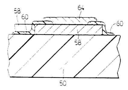
Referring now to Figures 5 and 6, a portion of a PCB 50 having a
contact 52 forming part of a low cost switch formed thereon in accordance with
the
present method is shown. Similar to conventional switches, the contact 52 is
used in
conjunction with a conductive elastomeric disc (not shown) to form the switch.
The contact includes a copper buss pattern 58 formed on selected areas
of the surface of the PCB 50. Soldermask 60 overlies the surface of the PCB 50
not
covered by the copper buss as well as areas of the copper buss 58. A window 62
is
defined by the soldermask to expose an area of the copper buss. TFP conductive
paste 64 covers the window 62 and a portion 66 of the soldermask 60 and
contacts
the copper buss 58.
~0~5148
With reference to Figures 7a to 7c, the steps involved in forming the
edge connector 30 are better illustrated. It should be apparent that when
forming the
contact 52, similar steps are used. When forming the edge connector 32, the
copper
buss 34 is applied to cover the selected areas of the substrate 30. Once this
is done,
the soldermask 36 is applied to the surface of the copper buss 34 in the areas
outside
of the window 38 as well as portions of the substrate not covered by the
copper buss
34. Thereafter, the TFP conductive paste 40 is applied to the upper planar
surface
34a of the copper buss 34 exposed by the window and over a small portion of
the
soldermask 36 via a machine screening process to form the electrically
conductive
edge connector 32.
Although the present method involves the additional step of covering
the portions of the copper buss not covered by the TFP conductive paste with
soldermask, this additional step does not present any problems since, as is
known to
those of skill in the art, the application of soldermask is used for other
reasons during
the manufacture of PCBs and, therefore, the addition of this step is easily
accommodated without increasing manufacturing costs.
Although the present method has been described as using a machine
screening process for the application of the TFP conductive paste on the upper
surface
of the copper buss, it should be realized that the TFP conductive paste may
also be
applied manually or by any other suitable application technique. In addition,
it should
be apparent to those of skill in the art that the present method contemplates
the use
of other types of conductive pastes and busses and should not be limited to
the use
of TFP conductive pastes and copper buss.
It should also be apparent to those of skill in the art that although the
present method has been described with reference to forming a single
electrically
conductive contact on a substrate, during typical manufacture of a PCB,
multiple TFP
screens are defined on the substrate at the same time and each of the
materials applied
~a~5148
_8_
to the substrate associated with each TFP screen are done so simultaneously so
that
after the last step, namely the application of the TFP conductive paste,
multiple
electrically conductive contacts are formed on the substrate simultaneously.
As should be appreciated, the present method of forming electrically
conductive contacts on a substrate is less complex than prior art techniques
thereby
simplifying the manufacturing process yet provides for the manufacture of
inexpensive
and reliable electrically conductive contacts.