Note : Les descriptions sont présentées dans la langue officielle dans laquelle elles ont été soumises.
2055802
COOLING STRUCTURE FOR ELECTRONICS DEVICES
BACXGROUND OF THE INVENTION
1. Field of the Invention
The present invention relates to a structure
for effectively discharging heat generated from
electronic devices out of an electronic apparatus on
which the former are mounted, such as a telecommunication
apparatus. Particularly, the present invention is
suitably applied to thin and small sized electronic
apparatuses of a type comprised of a single main printed
circuit board.
2. Description of the Related Arts
Recently, an electronic apparatus has been
small-sized in accordance with the development of LSI
technology. Accompanied therewith, removal of heat
generated from densified electronic devices out of a
system in which they are installed, has been a serious
problem. Particularly, in small-sized apparatuses with a
volume of less than 1~, and since there is no space for
providing a fan to forcibly cool the electronic devices,
it is necessary to adopt a natural cooling system.
As shown in Fig. 8(a) and 8(b), the conventional
cooling structure comprises a fin plate 23 common to
electronic devices 22 such as LSI mounted on a printed
circuit board 21. The fin plate 23 is positioned to be
in contact with the heat-conductive surface of the
electronic devices 22 and fixed on the printed circuit
board 21 by means of screws 26. Upper and lower springs
24, 25 are arranged around upper and lower halves of the
respective screw 26 so that close contact between the fin
plate 23 and the electronics devices 22 is enhanced,
while protecting the latter from the weight of the
former. Reference numerals 27, 28 designate,
respectively, a housing and a ventilation opening.
The above prior art cooling structure has the
following drawbacks:
- 2 - 2~ Z
1) A connection area between the printed circuit
board and the electronic devices mounted thereon is
liable to be damaged by vertical vibration caused by the
heavy fin plate supported in a floating manner above the
printed circuit board by the springs.
2) It is very difficult to bring all electronic
devices, such as LSI, into close and uniform contact with
the common fin plate, because said electronic devices
have inherent manufacturing dimensional errors in the
outer size thereof, to which a variation of solder
thicknesses in the connection area is further added.
This tendency is particularly promoted when the printed
circuit board has a curvature and a torsion. Of course,
this system cannot be adopted when at least one of the
electronic devices to be mounted on the printed circuit
board has a height different from the others.
3) The problems cited in item 2) can be solved by
providing a separate fin plate on the respective
electronic devices, but this results in a considerable
reduction of the mounting efficiency of the same.
4) The number of parts increases resulting in
higher manufacturing costs.
SUM~RY OF THE INVENTION
Accordingly, it is an object of the present
invention to solve the abovesaid drawbacks of the prior
art and to provide a novel cooling structure for
electronic devices mounted on a printed circuit board
that can be used even when the heights of the electronic
devices are somewhat different from each other.
This object is achieved by a cooling structure for
the electronic devices, such as LSI, mounted in the
electronic apparatus, comprising a main printed circuit
board mounting thereon first electronic devices with low
heat generation; at least an auxialiary printed circuit
board mounting thereon a second electronic devices with
high heat generation and connected with one edge of the
main printed circuit board through a flexible printed
- 3 - 2055802
circuit tape; a holder fixed on the main printed circuit
board for resiliently supporting the auxiliary printed
circuit board at a distance above the former when the
latter is turned over above the main printed circuit
board by bending the flexible printed circuit tape so
that a heat conductive surface of the second electronic
device mounted thereon is exposed outside; and a heat
conductive means tightly brought into contact with the
heat conductive surface of the second electronic device
for transferring heat from the second electronic device
to the outside.
Preferably, the heat conductive means is part of a
housing made of heat conductive material for
accommodating a printed board assembly consisting of the
main and auxiliary printed circuit boards and holders,
and is pressed onto the second electronic device when the
printed circuit board assembly is accommodated in the
housing.
Advantageously, the heat conductive means is a box-
like upper half body of the housing provided with aplurality of fins extended inward at a ridge line
thereof.
Favorably, the-upper half body of the housing has a
thicker inner wall portion at a position corresponding to
that of the second electronics device to enhance the heat
conductance contact therebetween.
BRIEF DESCRIPTION OF THE DRAWINGS
These and further objects and advantages of the
present invention will be more apparent from the
preferred embodiments illustrated in the attached
drawings; wherein
Fig. l(a) is a plan view of a straight printed
circuit board assembly according to the present
invention;
Fig. l(b) is a view in the arrowed direction of Fig.
l(a);
Fig. 2(a) is a plan view of a bent printed circuit
.
_-4 _ ~0~802
board assembly according to the present invention;
Fig. 2(b) is a view in the arrowed direction X of
Fig. 2(a);
Fig. 2(c) is a view in the arrowed direction Y of
Fig. 2(a);
Fig. 3(a) is a plan view of a holder for supporting
an auxiliary printed circuit board;
Fig. 3(b) is a sectional view along a line I-I of
Fig. 3(a);
Fig. 3(c) is a view in the arrowed direction of Fig.
3(a);
Fig. 4 is a side sectional view of the printed
circuit board assembly accommodated in a housing;
Fig. 5 is an exploded perspective view of a cooling
structure according to the present invention;
Fig. 6 is a partially broken perspective view of an
assembled cooling structure according to the present
invention; and
Fig. 7 is a side view of another cooling structure
according to the present invention;
Fig. 8(a) is a perspective view of the conventional
cooling structure; and
Fig. 8(b) is a sectional view along a line II-II of
Fig. 8(a)-
2S DESCRIPTION OF THE PREFERRED EMBODIMENTS
A principle of the present invention will be
explained with reference to Figures 1 through 4.
An electronic circuit package assembly according to
the present invention consists of a large size single
main printed circuit board 1 and four small size
auxiliary printed circuit boards 2, as shown in Fig. l(a)
and l(b). The number of auxiliary printed circuit boards
2 is not limited to four but must be at least one.
Electronic devices 3 are mounted on the main printed
circuit board 1, which generate less heat during the
operation thereof (hereinafter referred to as "first
electronic device'~) such as IC. While, an electronic
_-5 _ 2~55802
device 4 is mounted on the respective auxiliary printed
circuit board 2, which generates more heat during the
operation thereof (hereinafter referred to as "a second
electronics device") such as LSI.
The respective auxiliary printed circuit board 2 is
connected to either side area of the main printed circuit
board 1 by a flexible printed circuit tape 5 for a signal
transmission therebetween.
As shown in Fig. 2(a), 2(b) and 2(c), the auxiliary
printed circuit board 2 is turned over and is above the
main printed circuit board 1 while bending the flexible
printed circuit tape 5 in a U-shape, so that the heat
conductive surface of the second electronic circuit
device 4 is facing up.
The main printed circuit board 1 has a holder 6
shown in Fig. 3(a), 3(b) and 3(c) and consisting of a
cross-shaped spring member 6a made of stainless steel and
supported by a stand 6b of a square cross-section rigidly
fixed on the upper surface of the main printed circuit
board 1 by a rivet 7 or the like at a position
corresponding to the respective turned-over auxiliary
printed circuit board 2. The auxiliary printed circuit
board 2 is supported at the four corners by the tip ends
of the cross-shaped spring member 6a and positioned above
the main printed circuit board 1 in a floating manner.
Thus, an assembly A of printed circuit boards is formed.
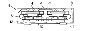
The assembly A is accommodated in a housing B
consisting of a box-Like upper half body 9 made of a
thermal conductive material, such as aluminum alloy,
having a plurality of fins 8 formed by perpendicular
incisions cut into a ridge line of the half body 9, as
shown in Fig. 5, and a plate-like lower half body 11 with
a plurality of ventilation slits 10 thereon.
As shown in Fig. 5 and 6, the main printed circuit
board 1 is fixedly secured by screws 13 on the respective
studs 12 protruding from the bottom wall of the lower
half body 11 at four corners thereof, while the
- 6 - 205~02
respective auxiliary printed circuit board is maintained
on the main printed circuit board 1 by the holder 6.
Then the upper half body 9 is capped thereon, whereby a
thicker area 14 is brought into contact with the heat-
S conductive surface of the second electronic device 4 andpushes the same downward against the elastic force of the
spring member 6a of the holder 6, which thicker area 14
is formed, corresponding to a position of the second
electronic device 4 mounted on the auxiliary printed
circuit board 2 on an inner surface of a top wall of the
upper half body 9. Accordingly, even though there is a
little height difference between the second electronic
device 4, it is absorbed by the elasticity of the spring
member 6a and close contact is assured between the
thicker area 14 and the respective second electronic
device 4 with a proper contacting pressure. Heat
generated from the second electronic device 4 is
effectively transmitted to the upper half body 9 and
radiated from the outer surface thereof by the fins 8
into the outer air.
As shown in Fig. 4, as the ridge line area of the
upper half body 9 becomes thicker, the outer surface of
the fins 8 formed in this area is large whereby effective
heat radiation is possible.
The first electronic device 3 having low heat
generation can be cooled by an air stream introduced from
outside into the housing A through the slits 10 caused by
natural convection, which air stream passes through the
incisions between the fins 8 and is discharged outside.
The cooling structure according to the present
invention has the following advantages compared with the
conventional structure:
1. As the auxiliary printed circuit board is held
above the main printed circuit board in a resilient and
floating manner by a special holder structure, the second
electronic device, having high heat generation, mounted
on the auxiliary printed circuit board can be brought
- 20S~80~
into close contact with the inner wall of the housing by
elastic pressure. Thereby even though there is a little
height difference between the respective electronic
devices mounted on the auxiliary printed circuit boards,
this difference is absorbed by the holder so that the
electronic devices can be always be brought into close
contact with the inner wall of the housing with
appropriate pressure.
2. According to the conventional cooling
structure, the fin plate is fixed directly on the heat
generating electronic device. According to the present
invention, the electronic device is resiliently pressed
onto the heat conductive means whereby the stress applied
to the soldered portion of the electronic device is
reduced and the same is not damaged.
3. As the housing has a wall thicker in the area
with which the electronic device is brought into contact
than that of the other areas thereof, the cooling effect
is enhanced due to the increased thermal capacity.
4. As the holder is fixed on the main printed
circuit board by a relatively thin stand at a center
thereof, a space occupied by the stand is very small,
whereby a space for mounting electronic parts on the main
printed circuit board is not substantially reduced.
The cooling structure according to the present
invention may be formed by combining a holder 6 with a
conventional fin plate 15 allocated to an individual
second electronic device 4, as shown in Fig. 7.