Note : Les descriptions sont présentées dans la langue officielle dans laquelle elles ont été soumises.
TITLE OF THE INVENTION 2 0 5 5 8 5 8
Holding Circuit
BACKGROUND OF THE INVENTION
Field of the Invention
The present invention relates to a holding circuit used
in a pedestal level clamp circuit of video signal of a color
television.
Related Art of the Invention
A holding circuit has a configuration in which a
capacitor is charged with a signal to be held. In the case
where this capacitor is built in an integrated circuit, since
its capacitance can not be increased above a certain degree,
various contrivances are necessary to improve holding
characteristics.
SUMMARY OF THE INVENTION
It is a first object of the present invention to
provide a holding circuit, in which a charge time constant is
substantially raised by including a circuit configuration
wherein base current being considerably smaller as compared
with collector current is used as the charging current of a
capacitor.
It is a second object of the present invention to
provide a holding circuit, in which inconveniences in the case
where the voltage to be held is lower than the reference
voltage are solved.
It is a third object of the present invention to solve
inconveniences in the case where PNP transistors and NPN
transistors are used together.
~,
- 2055858
It is a fourth object of the present invention to solve
inconveniences due to differences in individual transistor
characteristics.
According to the above objects, form a broad aspect,
the present invention provides a holding circuit comprising a
differential amplifier in which a reference voltage is applied
to a first input terminal and a voltage to be held is applied
to a second input terminal. A first transistor is also
provided and whose conducting state is controlled by current
which flows in response to a difference in two input voltages
of the differential amplifier. A second transistor is also
provided and whose collector current is directed by collector
current of the first transistor. A capacitor is connected
with the base of the second transistor at one terminal and
charged by the base current. A discharge circuit is connected
with the said one terminal of the capacitor.
The above and further objects and features of the
invention will more fully be apparent from the following
detailed description with accompanying drawings.
BRIEF DESCRIPTION OF THE DRAWINGS
Fig. 1 is a circuit diagram of a conventional holding
circuit;
Fig. 2 is a circuit diagram of a conventional holding
circuit having two discharging circuitsi
Fig. 3 is a circuit diagram of a first embodiment of
the present invention;
~,
- 2055858
_ Fig. 4 is a circuit diagram of a second embodiment of
the present invention;
Fig. 5 is a circuit diagram of a third embodiment of
the present invention, and
Fig. 6 is a circuit diagram of a fourth embodiment of
the present invention.
DESCRIPTION OF PRIOR ART
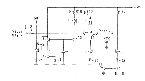
Fig. 1 is a holding circuit disclosed in Japanese
Patent Application Laid-Open No. 64-78008. In Fig. 1,
reference numeral 31 designates a differential amplifier in
which emitters of two NPN transistors, 14, 15 are commonly
connected on the ground side, and these emitters are connected
with a ground line via a transistor 16 and a resistance 17 for
switching. Serial circuit of a resistance Z0, a transistor 21
and a resistance 22 connected with a power terminal 24 is a
constant-current circuit. Bases of the transistors 21 and 16
are connected and a transistor 19 is connected between these
bases and the ground line. Clamping pulse is inputted to a
base 23 of the transistor 19, and when the clamping pulse is
"L", the transistor 16 is turned on. A reference voltage Vref
is applied to the base of the transistor 15 from a d.c. power
source 18. To the base of the transistor 14, for example,
video signal of NTSC are given from a terminal 1 via a
resistance 2. A capacitor 9 is charged from the power
terminal 24 via a resistance 10 and a transistor 11. A
collector of the transistor 14 is connected with a resistance
13, and the connecting point is given to the base of the
~,
2055858
_~ransistor 11. Transistors 6, 5 and 3 are in Darlington
connection, and a circuit connecting the base of the
transistor 6 to the capacitor 9 is a discharge circuit. An
emitter 5 of a transistor 3 in the final stage is connected
with the ground line via a resistance 4, and a collector is
connected with the connecting point of the resistance 2 and
the transistor 14, the connecting point serving as an output
terminal 50 of a holding circuit.
Since the pedestal level of the video signal inputted
is higher than the reference voltage Vref, when the clamping
pulse is given and the transistor 16 is ON, current flows
through the transistor 14, thereby the transistor 11 is turned
on and the capacitor 9 is charged by the collector current.
On the other hand, when the transistor 16 is OFF, the
capacitor 9 is discharged through the discharge circuit of the
transistor 6 and so on. By repeating such operations,
voltages of the transistor 14 base or the output terminal 50
becomes equal to the reference voltage Vref.
As such, in Japanese Patent Application Laid-Open No.
64-78008, since impedance of the discharge circuit is
increased by composing the discharge circuit of three
transistors connected in Darlington Connection, a discharge
time constant is large enough to compensate insufficient
capacitance of the capacitor.
In such a holding circuit, a large charge time constant
is also desirable. Namely, it is desirable to become
reference voltage Vref by a few number of H of the video
signal. This is because that if it is held at 1 or 2 H, the
~,
2055858
~_lamp level fluctuates by noises and images are unstable.
Therefore, it may be considered to increase the resistance
value of the resistance 10 in a charging circuit, but the
large resistance can not be controlled precisely in the
integrated circuit.
As another method, it may be considered to lengthen the
charging time by reducing collector current of the transistor
11. For this purpose, the resistance value of the resistance
17 may be increased to reduce the current flowing through the
transistors 14, 16. However, if it is arranged in such a
manner, the switching operation of the transistor 16 becomes
unstable and an accurate holding operation can not be
accomplished.
Meanwhile, there are other problems as to the
discharging circuit. In the case where noises are superposed
on a video signal, there are cases in which the base potential
or output voltage of the transistor 14 may become lower than
the reference voltage Vref. When the output voltage becomes
lower than the reference voltage Vref as such, current does
not flow to the transistor 14 side, and not only the capacitor
9 is not charged, potential rise of the output terminal 50
delays due to the high discharge time constant. Namely, when
the charge time constant is small and susceptible to the
influence of noises, the large discharge time constant may
cause inconveniences.
Fig. 2 shows a circuit in which another discharge route
is added to solve such problems. Serial circuit of
transistors 25, 26 is connected between the power terminal 1
~,
2055858
_~nd the ground line, and a collector of the transistor 15 is
connected with the transistor 25 base. To the transistor 26,
a transistor 27 is connected with a Mirror circuit therewith,
and a collector of the transistor 27 is connected with a
terminal of the capacitor 9.
When such a circuit is provided, the transistors 25, 26
are turned on when the transistor 15 is ON, and current same
as those flowing through the serial circuit flows to the
transistor 27 and serves as a discharge current of the
capacitor, thereby the problems may be solved for the time
being but the holding voltage fluctuates relatively violently,
and when used in a pedestal clamp circuit, the stability of
images is spoiled.
DESCRIPTION OF THE PREFERRED EMBODIMENT
Fig. 3 is a circuit diagram of a first embodiment of
the present invention. In Fig. 3, reference numeral 31
designates a differential amplifier, and emitters of two NPN
transistors 14, 15 are connected commonly. These emitters are
connected with a ground line via an NPN transistor 16 for
switching and a resistance 17. Serial circuit of a resistance
20, an NPN transistor 21 and a resistance 22 connected with a
power terminal 24 is a constant-current
B
2~ 8S~3
circuit. Bases of the transistors 21, 16 are connected and
between these bases and the ground line, an NPNtransistor
19 is connected. Clamping pulse is inputted to a base 23 of
the transistor 19, and the transistor 16 is turned on when
this is "L". To the transistor 15 base, the reference
voltage Vref is applied from a d.c. power source 1~.. To the
transistor 14 base, video signal of NTSC, for example, is
given from a terminal 1 via a resistance 2. Between the
power terminal 24 and the ground line, a serial circuit of a
resistance 10 and PNP transistors 11, 12 is provided. The
transistor 11 base is connected with a collector of the
transistor 14, and a resistance 13 is connected between the
connecting point and the power terminal 24. A capacitor 9
is connected between the transistor 12 base and the ground
line, and is charged by base current of the transistor 12.
NPN transistors 6, 5 and 3 are in Darlington connection, and
a circuit connecting the transistor 6 base to the capacitor
9 is a discharge circuit. An emitter 5 of the transistor 3
in the final stage is connected with the ground line via a
resistance 4, and a collector is connected with the connect-
ing point of the resistance 2 and the transistor 14, the
connecting point serving as an output terminal 50 of a
holding circuit.
Next, the operation of the circuit will be described.
It is different from the circuit of Fig. 1 in that, the
-
2~ 3S~3
capacitor 9 is not charged by collector current of the
~ransistor 11 but by base current of the transistor 12
directed by the collector current.
Since a pedestal level of the video signal inputted is
higher than the reference voltage Vref, current flows to the
transistor 14 when the clamping pulse is applied and the
transistor 16 is ON, thereby the transistor 11 as well as
the transistor 12 are turned on. Collector currents of the
transistors 11 and 12 are equal. ~hen the collector
current, emitter ground current amplification factor of the
transistor 12 and base current thereof are denoted respect-
ively as Ic, ~ and Ib, the following equation is obtained.
Ib = Ic/(l + ~) . Ic/~
Contrary to the circuits in Figs. 1 and 2 where charging is
effected by Ic, in the present invention, charging is
effected by Ib. Assuming that ~ takes a value of about
100, in this invention, charging current becomes smaller by
that much and the charging time constant becomes larger.
Thereby, it is possible to restrict influence of noises.
Thus, when used in a pedestal level clamp circuit, stable
images can be accomplished.
The capacitor 9 is discharged in the same manner as the
conventional circuit shown in Fig. 1.
Fig. 4 shows a differential amplifier 31 which is
constituted by PNP transistors 14, 15. Emitters of the
205S8S8
transistors 14, 15 are connected commonly and connected with
a power terminal 24 via a PNP transistor 16 and a resistance
17. A collector of the transistor 15 to which the reference
voltage is applied is connected with the ground line via a
resistance 130.
With connecting point of the resistance with the
collector of the transistor 15, the base of an NPN tran-
sistor 110 is connected, and an emitter of the transistor
110 is connected with the ground line via a resistance 100.
A collector of the transistor 110 is connected with the
power terminal 24 via a PNP transistor 28 and a resistance
30. A serial circuit of a PNP transistor 29 and a
resistance 32 is connected with a serial circuit of the
transistor 28 and the resistance 30 to constitute a Mirror
circuit, and a collector of the transistor 29 is connected
with an emitter of a PNP transistor 12. It is same as the
circuit shown in Fig. 3 that the base of the transistor 12
is connected with the capacitor 9.
A discharge circuit is exactly as same as those shown
in Fig. 3. Portions to which clamping pulse is inputted are
all provided with the PNP transistors 19, 21 corresponding
to the fact that the transistor 16 is a PNP transistor.
These portions are designated by reference numerals
corresponding to those in Fig. 3 and their e~planation is
omitted.
, ~
~055~58
When the transistor 16 is turned on by the clamping
pulse, the transistor 15 on the reference voltage Vref side
and lower than the input signal level is turned on. There-
by, the transistor 110 is On and current equivalent to the
collector current flows through the circuit of transistors
29 and 12. Thereby, current of 1/~ of this current flows
to the transistor 12 base and serves as the charging current
of the capacitor 9.
- Fig. 5 shows a third embodiment of the present
invention, in which another discharge circuit is added to
the second embodiment. A collector of the transistor 15 on
the reference voltage input side is connected with the
ground line via a serial circuit of an NPN transistor 38 and
a resistance 39. This serial circuit-is connected with a
serial circuit of a transistor 110 and a resistance 100 to
constitute a Mirror circuit. A collector of the transistor
14 to which the voltage to be held is inputted is connected
with the ground line via a serial circuit of an NPN
transistor 35 and a resistance 37. This serial circuit is
connected with a serial circuit of an NPN transistor 34 and
a resistance 36 to constitute a Mirror circuit. A collector
of the transistor 34 is connected with an emitter of an NPN
transistor 33. A collector of the transistor 33 is
connected with the power terminal 24 and a base thereof is
connected with the capacitor 9.
~ . .
~ -a
z~ s~
In the case where the input voltage to the differential
amplifier 31 is higher than the reference voltage Vref, the
transistors 15, 38 side are turned on and the equivalent
current flows to the transistor 110. Conversely, in the
case where the input voltage is lower, the transistors 14,
35 are turned on and the equivalent current flows to the
transistors 33, 34. When collector current of the transist-
ors 33, 34 and emitter ground current amplification factor
of the transistor 33 are denoted respectively as Ic and ~,
base current of the transistor 33 becomes Ic/~.
Namely, in the third embodiment, in case of the low
voltage input, though the capacitor 9 is discharged from the
transistor 33 side, since it becomes discharge current of
1/~ of the circuit of Fig. 2, the output voltage is
restored gradually. Thus, when used in a pedestal clamp
circuit, stability of images is improved.
Now, the circuit of Fig. 5 will be examined in detail.
Correctly speaking, the differential amplifier 31 is not
valanced when its two input voltages become equal, but is
balanced in the state where charging and discharging
currents of the capacitor 9 are equal. These currents are
respectively base currents of the transistors 12, 33. These
base currents are collector current of the transistor 12
itself or the transistor 110, and collector current of the
transistor 33 itself or the transistor 34. Though circuits
-
35~3
to the transistors 110, 34 are symmetrical on the transist-
ors 14, 15 sides, the transistors 12, 33 are respectively
the PNP and NPN type and in case of Ic, ~ of two types do
not coincide. Therefore, in the circuit of Fig. 5, some
difference is generated between the charging and discharging
currents and the output voltage is stabilized in the state
having offset from the reference voltage.
Fig. 6 shows an embodiment in which such inconvenience
has been solved. It is different from the circuit shown in
Fig. 5 in that, in place of the PNP transistor 28 an NPN
transistor 280 is used. In this embodiment, with a circuit
of a resistance 22 and a transistor 21, which supplies
constant current, an NPN transistor 41 is connected in
series, and a micro-constant-current source 40 is connected
with its base.
When current I is applied from the micro-constant-
current source 40, collector current of ~NI flows through
the transistor 41. ~N is an emitter ground current
amplification factor of the NPN transistor. This current
flows also to a transistor 21 which is in series with the
transistor 41, and to a transistor 16 which constitutes a
Miller circuit with the transistor 21. When the rate of
current flowing to the transistor 14 side is A (_1),
currents flowing respectively through the transistors 14, 15
become A~NI and (1 - A)~NI. The current (1 - A)~NI flows
12
-
Z~5~8~3
also to a transistor 38 which is in series with the
transistor 15, to a transistor 110 which constitutes a
Miller circuit with the transistor 38 and further to a
transistor 280 which is in series with the transistor 110.
Meanwhile, the current A~NI flows also to a transistor
35 being in series with the transistor 14, to a transistor
36 constituting a Miller circuit with the transistor 35 and
to a transistor 33 being in series with the transistor 36.
Base current of the transistor 280 is l/~N of the
collector current (1 - A)~NI, thus it becomes (1 - A)I.
When ~P is an emitter ground current amplification factor
of the PNP transistor, collector currents of the transistors
29, 12 become (1 - A) ~Pl . Thus, base current of the
transistor 12 or ch~rging current of the capacitor 9 becomes
( 1 - A)I.
On the other hand, since the collector current of the
transistor 33 is A~NI as stated above, its base current or
discharging current of the capacitor 9 becomes AI.
In such an embodiment, since charging and discharging
currents of the capacitor 9 are independent of the
difference of amplification factor of the PNP and NPN
transistors, A becomes roughly 0.5. Thus, the afore-
mentioned problem of offset is solved. Furthermore, in this
embodiment, since ~N and ~P are independent of the
charging and discharging currents, variations in charging
2~C~8S~
and discharging currents of individual IC are eliminated.~
In the embodiment of Fig. 6, though the micro-constant-
current source 40 and the transistor 41 are provided and
current of the differential amplifier 31 is ~NI, in the
case where the constant-current circuit of the transistor 21
and the resistances 20, 22 are employed without the micro
constant current source 40 and the transistor 41 as shown in
Figs. 4 and 5, when the current is Ic, current of the
differential amplifier 31 also becomes Ic. Thus, according
to the aforesaid description, the charging current becomes
(1 - A)Ic/~N and the discharging current becomes AIc/~N.
Here, though the problem of characteristic fluctuation of
individual Ic due to variations in ~N may exist, the
problem of offset due to difference according to
amplification factor of the PNP and NPN transistors is
solved.
A holding circuit of the present invention may be
applied in an automatic gain control circuit and an
automatic color control circuit of a color television.
As this invention may be embodied in several forms
without departing from the spirit of essential characteris-
tics thereof, the present embodiment is therefore illustra-
tive and not restrictive, since the scope of the invention
is defined by the appended claims rather than by the de-
scription preceding them, and all changes that fall within
z~ sa
the metes and bounds of the claims, or equivalence of such
metes and bounds thereof are therefore intended to be em-
braced by the claims.