Note : Les descriptions sont présentées dans la langue officielle dans laquelle elles ont été soumises.
- 1- 2055~8
1 Optical Modulating Device
8ACKGROUND OF THE INVENTION
Field of the Invention
The present invention relates to an optical
modulating device employing an material having an
anisotropy of refractive index, and particularly,
to an optical modulating device employing
ferroelectric liquid crystals (referred to as "FLC"
hereinafter) showing the anisotropy of refractive
index. Such an optical modulating device is
preferably used in a display apparatus which displays
letters, characters or images.
Related Background Art
One mode of an optical modulating device
(SSFLC) in which a ferroelectric liquid crystal
layer is formed in a narrow gap (e.g. 1 to 2 ~m)
between a pair of parallel boards and in which the
surface effect of the boards provides bistability for
the FLC (described in Appl. Phys. Lett. 36 (1980)
899) has been expected to provide a wide range of
application because of its quick response and memory
effect.
The bistable FLC device shows two stable
states in directions shifted a certain angle both
ways from the axis direction (rubbing direction or
the like) of the aligning surface, which is formed
- 2 - 2055868
1 by a rubbing method or the like on the liquid-
crystal-side surfaces of boards positioned on both
sides of the liquid crystal layer. The tilt angle
is called a cone angle (hereinafter referred to by
S 0c). When voltage is applied perpendicularly to the
liquid crystal layer of the FLC device, the FLCs shift
from one stable state to the other. This shift
corresponds to the 20c rotation on a plane of the FLC
layer of the principal axis of index ellipsoid of a
material having anisotropy of refraction index.
Although, strictly speaking, the main axis of the
index ellipsoid does not always coincide with axis of
the liquid crystal molecules, it is supposed that
the two axis are in the same direction, to simplify
the descripticn. Therefore, when polarized light
comes into a bistable FLC device having a thickness
corresponding to the operation of a halfwave plate,
the rotating effect of polarization to the incoming
polarized light in one of the two stable states is
40c different from that in the other. When such a
bistable FLC device is placed between polarizers
(such as polarizing plates) positioned in crossed
nicols or parallel nicols, an ON/OFF ratio of
transmitted-light quantity, i.e., transmittance
ratio, contrast, between the two stable states
reaches a maximum if
4~c = 90 (~c = 22.5).
_ 3 _ 20S~868
l Fig. 4 illustrates an FLC device having
polarizing elements positioned in crossed nicols.
In the figure, incident light Ein goes through a
polarizer 1 to become polarized light El, which goes
into an FLC layer 2 having an effect equivalent to
that of a halfwave plate. The direction of the
polarization of the incident light E1 is the same as
that of the axis 45 of the FLC molecules in one of
the two stable state. An analyzer 3 is positioned
perpendicular to the polarizer 1. Another FLC
molecule axis 46 is that of the other stable state.
The molecule axes 45 and 46 have cone angles of +~c
and -~c, respectively, to an aligning axis 44, for
example, determined by the rubbing method. When the
FLC molecules are in one stable state 45, the
polarized light is not rotated by the FLC layer 2
and thus entirely blocked by analyzer 3. Black is
thus expressed. When the FLC molecules are i~ the
other stable state 46, the polarized light is rotated
40c by the FLC layer 2, and then it is transmitted
by the analyzer 3 at a ratio of
sin (4~c)
white is thus expressed.
Cone angles ~c in bistable FLC devices are
substantially dependent on temperature. Thus, even
if a device is positioned as shown in Fig. 4 at one
temperature, the FLC molecule axis 45 in one of the
4 255868
two stable states tilts from the polarization direction
of incident light at another temperature because of a
change in cone angle. In such a case, the polarized
light is rotated by the polarization effect of the FLC
layer. Therefore, the contrast degrades because black is
not fully expressed in the case where the polarizer 1 and
the analyzer 3 are positioned in crossed nicols, or
because white is not fully expressed in the case where
they are positioned in parallel nicols.
SUMMARY OF THE INVENTION
It is an object of the present invention to
solve the above mentioned problems by providing an
optical modulating device in which contrast degradation
is substantially reduced.
In order to achieve the object, the present
invention provides an optical modulating device which
comprises a polarizer, an analyzer, and liquid crystals
with an aligning axis positioned between the polarizer
and the analyzer, and which controls the birefringence of
the liquid crystal by applying an electric field to the
liquid crystals so as to change the light polarization
direction of the device, and which further comprises a
rotatable halfwave plate being positioned between the
liquid crystals and the analyzer or between the liquid
crystals and the polarizer in such a manner
_ 5 _ 2055868
that the optical axis of the halfwave plate will be
rotated around the optical axis of a display apparatus
employing the optical modulating device and the
aligning axis of said liquid crystals, and wherein the
rotational angle of the halfwave plate is varied in
accordance with the temperature of the liquid crystals
or the environment thereof, and particularly such
angles have one-to-one correspondence to such
temperature.
In the construction as described above, when
a proper corresponding relation is set between the
rotational angle of the halfwave plate and the
temperature of the liquid crystals or its environment,
the display conditions in one of the two stable states
of the liquid crystals are not affected by a change in
cone angles caused by the temperature change. In other
words, a constant transmittance can be maintained.
Ferroelectric liquid crystals (FLCs) are used
as the liquid crystals.
An optical modulating device according to the
present invention may have one of two main
constructions. In the first construction, the
transmission axes of the polarizer and the analyzer are
perpendicular to each other, and the transmission axis
of the polarizer is parallel to the FLC molecule axes
in one of the two stable states of the FLCs. In the
second construction, the transmission axes
- 6 - 205S868
1 Of the polarizer and the analyzer are parallel to
each other, and as in the first construction, the
transmission axis of the polarizer is parallel to the
FLC molecule axes in one of the two stable states
of the FLCs. In either construction, in one of the
two stable states, the affection which a cone angle
of the FLCs shifted by a temperature change has onto
the polarization of the incoming light is cancelled
by the polarization effect provided by the
accordingly tilted halfwave plate, and thus the
direction in which incident light is polarized is
not rotated, in total, by the polarization. Thus,
in one of the two stable states of the FLCs, complete
black or complete white can be expressed in spite
of the temperature change, so that images with a
high contrast can be displayed.
BRIEF DESCRIPTION OF THE DRAWINGS
Fig. 1 is a schematic sectional view of an
optical modulating device according to an embodiment
of the present invention;
Fig. 2 is a schematic perspective view of the
optical modulating device shown in Fig. 1,
illustrating the state of each layer thereof at a
standard temperature.
Fig. 3 is a schematic perspective view of
the optical modulating device shown in Fig. 1,
- 7 - 20~5868
l illustrating the state of each layer thereof at a
temperature other than the standard temperature; and
Fig. 4 is a schematic perspective view of
a conventional optical modulating device,
illustrating the staté of each layer thereof.
DETAILED DESCRIPTION OF THE PREFERRED EMBODIMENTS
Embodiments of the present invention will
be described hereinafter with reference to the
figures.
[Embodiment 1]
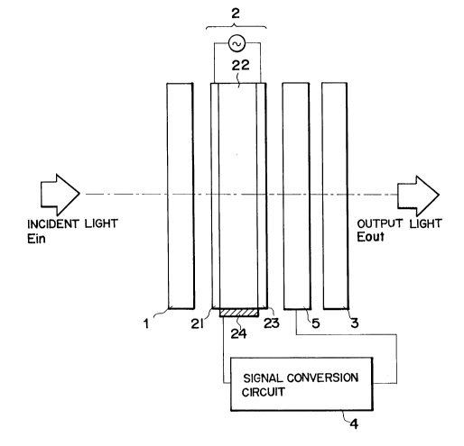
With reference to Fig. 1, a polarizer 1
linearly polarizes incident natural light. An FLC
layer 2 controls the state of polarization of
incoming linearly polarized light (modulates the
light) in accordance with an applied voltage. An
analyzer 3 transmits only a component of the light
modulated by the FLC layer 2, such component having
a specified direction. A signal conversion circuit
4 includes a ROM storing a table in which rotational
angles correspond to temperatures. A halfwave plate
5 is rotatable. The FLC layer 2 is composed of a
pair of transparent base boards 21 and 23 facing
each other, an FLC molecule layer 22 provided between
the base boards 21 and 23, and a temperature detector
24 of the FLC molecule layer 22.
Incident light is linearly polarized by the
- 8 - 205~868
l polarizer l and then is modulated by FLC 2. After
the modulated light goes through the halfwave plate
5, it goes into the analyzer 3, which transmits only
a component light in the transmission direction
thereof. The FLC molecule layer 22 exhibits one of
the two stable states according to the direction of
the electric field applied thereto by transparent
electrodes (not shown~ formed on the insides of the
base board 21 and 23.
The temperature detector 24 detects the
temperature of the FLC molecule layer 22 and its
environment. The temperature values are converted
by the signal conversion circuit 4 into signals whcih
control the rotation of the halfwave plate 5.
Figs. 2 and 3 illustrate the state of each
layer of the optical modulating device at different
temperatures A and B, respectively. In the figures,
44 denotes an aligning axis for the FLC molecu-les,
and the angles spreading clockwise with respect to
the direction in which the light along the optical
axis travels are expressed by negative values.
Referring to Fig. 2, FLC molecules axes 45
and 46 in the two stable states are at once angles
+~c and -~c respectively to the aligning axis 44 at
the temperature A. Incident unpolarized light Ein
is polarized by the polarizer 1, so that the
polarized light goes into the FLC layer 2 with
- 9 - 20SS868
1 the polarization direction of the light being in the
direction of the molecule axis 45 at the cone angle
+~c. When no electric field is applied to the FLC
layer 2, the FLC molecule axis is in the direction
45. In such a case, the polarized light is not
rotated by the polarizing effect of the FLC layer 2,
nor by the polarizing effect of the halfwave plate 5,
and then is entirely blocked by analyzer 3. Thus,
complete black is expressed. When an electric field
is applied to the FLC layer, the FLC molecule axis
is in the direction 46. In this case, the polarized
light is rotated -40c by the FLC layer 2 having an
effect equivalent to that of a halfwave plate, and
then is rotated 8~c by the halfwave plate 5. Thus,
the total polarizing rotation by the FLC layer 2 and
the halfwave plate 5 is 4~c. Therefore, as in the
conventional art, the light is transmitted by the
analyzer at a ratio of
sin (40c).
Referring to Fig. 3, when the temperature
of the FLC is B, FLC molecule axes 42 and 43 in the
two stable states are at cone angles +Oc' and -~c'
respectively to the aligning axis 44, and the
halfwave plate 5 is rotated -(Oc - Oc') from the
position thereof at the temperature A shown in Fig.
2. As in the case where the temperature is A,
incident unpolarized light is polarized by the
lO- 20~68
1 polarizer 1, so that the polarized light goes into
the FLC layer 2 with the polarization direction of
the light being in the direction 45 (shown in Fig. 2),
which is at an angle Oc to the aligning axis 44.
When no electric field is applied to the FLC layer
2, the FLC molecule axis is in the direction 42. In
such a case, the polarized light is rotated -2(0c -
Oc') across the molecule axis 42 by the polarizing
effect of the FLC layer, and then is rotated 2(~c
Oc'), in the opposite direction, by the polarizing
effect of the halfwave plate 5, which is rotated
-(Oc - ~c') as described above. The two polarizing
rotations offset each other. Therefore, the light
coming out of the halfwave plate is entirely blocked
by the analyzer 3. Thus, complete black is
expressed. When an electric field is applied to the
FLC layer 2, the FLC molecule axis is in the
direction 43. The polarized light is rotated ~2(0c'
+ ~c) by the FLC layer 2, and then is rotated
(6~c' + 2~c) in the opposite direction by the
halfwave plate 5. Thus, the total polarizing
rotation hecomes 40c'. Thus, the total polarizing
rotation becomes 40c'. The light is transmitted by
the analyzer at a ratio of
sin (40c'),
As described above, black is expressed in the
constant state in spite of the temperature change.
11- 20~5868
1 Thus, an optical modulating device according to this
embodiment provides high-quality images with a high
contrast in a wide temperature range.
An element in the signal conversion circuit
is not necessarily a ROM but may be another element
having functions equivalent to those of the ROM.
~Embodiment 2]
This embodiment differs from the embodiment
1 in that a polarizer 1 and an analyzer 3 are
positioned so that the transmission axes thereof are
parallel with each other and are parallel with the
FLC molecule axis in one of the two stable states.
The incoming polarized light is rotated by
the polarizing effect of the FLC layer and the
halfwave plate in the same manner as in the
embodiment 1. When there is no electric field
applied to the FLC layer, the analyzer 3 transmits
the polarized light entirely. Thus, complete white
is expressed. The direction of the polarization
completely coincides with the transmission axis of
the analyzer, in spite of the temperature change.
Thus, this embodiment provides an optical
modulating device which displays high-quality images
with a high contrast in a wide temperature range.
Although the polarizer and the analyzer in
the embodiment 1, 2 are perpendicular or parallel
to each other respectively, they may be positioned
- 12 - 2~ 68
l in other manners providing effects similar to those
in the embodiments.,
[Embodiment 3]
According to this embodiment, the FLC layer 2
and the halfwave plate 5 in the embodiments 1, 2 may
be interchanged in position. As in the above
embodiments, this embodiment provides an optical
modulating devic_ which expressed complete black or
complete white, i.e. displays high-quality images
with a high contrast, in a wide temperature range.
LEmbodiment 4]
According to this embodiment, the rotatable
halfwave plate 5 in the above embodiments is sub-
stantially a circle which externally touches the four
corners of the quadrangular-shaped FLC layer 2, or it
is substantially a quadrangle which externally touches
such a circle. In this manner, all the light coming
out of the FLC layer 2 goes into the halfwave pLate 5,
or all the light coming out of the halfwave plate 5
goes into the FLC layer 2 in the case where they are
positioned as in the embodiment 3.
Although the present invention is applied to
an optical modulating device using bistable FLCs in
the above description, the present invention may be
applied to optical modulating devices which are
other types of liquid crystals since such devices
have substantially the same problems as described
- 13 - 205~868
l above. In such cases, the present invention will
provide substantially the same effect as described
above.
Being constructed as described above, an
optical modulating device according to the present
invention provides a constant contrast or a high
transmittance in spite of a change in the temperature
of the FLC layer and thus displays high-quality
images.