Note : Les descriptions sont présentées dans la langue officielle dans laquelle elles ont été soumises.
- AE-364 2 0 59386
SOCKET AND HEADER ELECTRICAL CONNECTOR ASSEMBLY
1 FIELD OF THE INVENTION:
The present invention relates to a connector
assembly including an interconnectable socket connector
and header connector. More particularly, the present
invention relates to a connector assembly for electrically
connecting an electronic apparatus housed in a socket
connector to a header connector.
BACKGROUND OF THE INVENTION:
In establishing electrical connection between
various components, especially in the electronics
environment, socketing has long been used as an expedient.
Socketing entails providing a pair of connectors which are
matable. One connector of the pair typically houses an
electronic apparatus while the other connector of the pair
is mounted and electrically secured to an object to which
connection is desired such as a printed circuit board.
Where connection is desired between an electronic
apparatus and a printed circuit board, the first connector
is usually referred to as a socket connector while the
second connector is usually referred to as a header
connector.
In addition to providing ease of
interconnectabilityj the socket connector is also used to
provide physical protection to the electronic apparatus
housed therein. Socket connectors may be constructed
which totally enclose an electronic apparatus housed
therein to prevent external contaminants from adversely
affecting the electrical performance of the apparatus.
However, in certain extremely harsh environments, such as
those found in the engine compartment of an automobile,
merely covering the electronic apparatus may be
insufficient protection.
- 205938~
1 The art has seen the use of encapsulation
techni~ues where the electronic apparatus is encapsulated
or potted, with a curable potting compound. The potting
compound is typically provided in a fluid state, which
after being poured around the electronic apparatus,
hardens or cures to a solid state, thereby providing an
environmental seal around the electronic apparatus.
Socket connectors, which support such electronic
apparatus, must be also capable of containing a curable
potting compound in such a manner that complete
encapsulation of the electronic apparatus is achieved.
In order to facilitate mass production of such
socketed connectors, the socket connector should support
the electronic apparatus in such a manner that it is
relatively easy to co~pletely encapsulate with potting
material.
SUMMARY OF THE IN~ TION:
It is an object of the present invention to
provide a connector assembly for electrically connecting
an electronic apparatus to a printed circuit board.
It is a further object of the present invention
to provide a socketable connector assembly which permits
the matable interconnection of electronic co~-ponents.
It is a still further object of the present
invention to provide a connector assembly for electrically
connecting an electronic apparatus supported in a socket
connector to a header connector supported on a printed
circuit board, and which permits the encapsulation of the
electronic apparatus supported in the socket connector.
In the efficient attainment of these and other
objects, the present invention provides a connector
assembly for electrically connecting an electronic
apparatus to a printed circuit board. The assembly
includes a socket connector and a matable header
connector. The socket connector includes an insulative
open-sided container which is capable of retaining a
curable potting compound. A plurality of electrical
205938~
1 contacts are supported by the container having first ends
within the container which engage and support the
electronic apparatus. Opposed second ends of the contacts
extend exteriorly of the connector. Means is provided for
supporting the electronic apparatus in a position within
the container to permit the electronic apparatus and the
first ends of the contacts to be surrounded by the potting
compound. A cover is supportable over the container to
enclose the potted electronic apparatus. The header
conne~tor is securable to the printed circuit board and
includes a-n insulative housing and plural electrical
terminals electrically engageable with the socket contacts
to establish electrical connection therebetween.
As more particularly shown by way of the
preferred embodiment, the socket connector includes an
open-sided container having a bottom wall and an
upstanding side wall extending around the perimeter of the
bottom wall. A support platform extends from the bottom
wall of the container to support the electronic apparatus
2~ in a position spaced from the bottom wall to permit the
potting compound to flow therearound. The first ends of
the contacts in the socket connector are positioned at a
location spaced from the botto~ wall and the side wall to
help support the electronic apparatus in a position where
the potting co~pound can easily flow therearound.
BRIEF DESCRIPTION OF THE DRAWINGS:
Figure 1 shows in exploded perspective view, the
socket connector of the connector assembly of the present
lnvention .
Figure 2 is a perspective showing of a header
connector of the connector assembly of the present
invention.
Figure 3 shows an electrical contact used in the
socket connector shown in Figure 1, attached to an
electronic apparatus.
20S9386
1 Figure 4 shows the socket contact and the
electrical apparatus shown in Figure 2, supported by a
housing of the socket connector of Figure 1.
Figure 5 shows partially in section, the
S assembled socket connector of Figure 1.
Figure 6 shows partially in section, the
asse~bled socket connector of Figure 5 inverted and
connected to the header connector shown in Figure 2.
DETAILED DESCRIPTIO~ OF THE PREFERRED EMBODIMENTS:
The electrical connector assembly 1 of the
present invention is shown in Figures 1 and 2. Connector
assembly 1 includes a socket connector 10 shown in Figure
1 and an intermatable header connector 12 shown in Figure
2. Socket connector lQ is formed of a suitable
electrically insulative plastic material and as shown in
Figure 1 includes a lower housing 14 and an upper cover
16. Lower housing 14 is generally rectangular in shape
having a planar bottom wall 18 and an upstanding side wall
20 extending about the perimeter of bottom wall 18. The
upper surface of lower housing 14 is open thereby forming
an open-ended container which is closed by cover 16.
Lower housing 14 and side wall 20 define and internal
cavity 21.
Socket connector lQ further includes plural
electrical contacts 22, one of which is shown in Figure
1. Contacts 22 are positioned on lower housing 14 in a
manner which will be described in further detail
hereinbelow.
Cover 16 is also generally rectangular in shape,
having a planar upper wall 24 and a depending side wall
26 extending perimetrically around upper wall 24. Cover
16 is constructed to fit over lower housing 14 to enclose
cavity 21 thereof. Cover 16 includes an upwardly
extending portion 28, which permits accommodation of
contacts 22 as will be described in further detail
hereinbelow. Cover 16 also includes a latch 30 mounted
on side wall 20. Latch 30 is manually operable to secure
-- 5 --
21~Sg386
1 ald lock socket connector 10 to header connector 12, as
will be described in further detail hereinbelow.
Referring additionally to Figure 3, socket
connector 10 is designed to house an electronic apparatus
32 which may include a printed circuit board 34 upon which
are mounted various electronic devices 36. Electrical
contacts 22 are used to establish electrical connection
with electronic apparatus 32. Contacts 22 are elongate
members form~d of suitably electrically conductive
material, and include a first end conventionally formed
into a pin receiving socket 38. Each contact 22 further
includes an elongate central portion 40 extending from
socket 38 to a connecting clip element 42 at the opposite
end thereof. Clip element 42 is used to engage an edge
1~ 34a of printed circuit board 34. Clip element 42 includes
upper and lower fingers 44 which engage opposed surfaces
of printed circuit board 34 about edge 34a. Fingers 44
typically electrically engage metallic traces (not shown)
OIl the surfaces of printed circuit board 34 to establish
,0 electrical connection therebetween. Central portion 40
of contact 22 includes an angled transition region 46
which horizontally spaces clip element 42 from socket 38.
In the present embodiment, it is contemplated
that socket connector 10 will employ eight contacts 22.
The contacts 22 are spaced along edge 34a of printed
circuit board 34. The clip elements 42 of contacts 22
secure contacts 22, both mech~nically and electrically to
printed circuit board 34. It of course may be appreciated
that a socket connector may be constructed which could
~0 support a various number of contact 22 as may be needed
for a particular application.
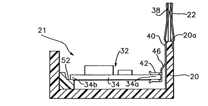
Referring now to Figure 4, the electronic
apparatus 32 and contacts 22 which are secured thereto,
are inserted into lower housing 14. Socket contact 22
includes a wall engaging portion 48, shown in Figure 3,
which clips onto an upper edge of 20a of side wall 20.
Tl~e engagement of each of contacts 22 with the upper edge
~ 2059~86
1 20a of side wall 20 secures the contacts thereto and also
fixably supports electronic apparatus 32 within cavity 21
of lower housing 14.
Contacts 22 are constructed so that central
portion 40 thereof extends down toward bottom wall 18, but
terminates in clip element 42 at a location spaced from
botto~ wall 18. Thus, as shown in Figure 4, clearance is
provided between printed circuit board 34 and bottom wall
18. Additionally, as shown in Figures 1 and 4, lower
housing 14 includes a platform 50 extending upwardly from
bottom wall 18 at a location spaced from contacts 22.
Platform 50 includes a board bearing surface 52, which is
substantially parallel to bottom wall 18 and which
supports an edge 34b of printed circuit board 34 opposite
to edge 34a. Platform 50 helps support printed circuit
board 34 within cavity 21 at a location spaced from bottom
wall 18. In addition, as particularly show in Figure 4,
transition region 46 of contact 22 disposes clip element
42 at a location spaced inwardly from side wall 20. This
provides a clearance between clip element 42 and side wall
20. Further, board bearing surface 52 of platform 50 is
spaced inwardly from side wall 20. Thus, as positioned
in Figure 4, printed circuit board 34 is positioned
centrally within cavity 21 spaced from side walls 20. By
spacing printed circuit board 34 away from both botto~
- wall 18 and side wall 20 of lower housing 14, clearance
is provided on all sides of printed circuit board 34 which
permits complete encapsulation of electric apparatus 32.
Referring now to Figure 5, as electronic
3Q apparatus 32, including printed circuit board 34, is
spaced both vertically and horizontally away from bottom
wall 18 and side wall 20 of lower housing 14, a potting
compound 56 may be poured into cavity 21 of lower housing
14 to completely surround electronic apparatus 32 as well
as clip ele~ents 42 of contacts 22 which engage printed
circuit board 34. Potting compound 56 is of the type
_ ~ 7 ~ 20 S 9386
1 which is commonly used and commercially available in the
electronics industry to environmentally seal electronic
components. It is typically provided in a fluid state so
that it may be poured into cavity 21 of lower housing 14,
to flow completely around electronic apparatus 32 and clip
elements 42 of contacts 22. The potting compound 56 is
permitted to cure to a hardened state whereby the
electronic apparatus as well as its electrical connection
to contacts 22, are environmentally sealed.
13 Once potting compound 56 hardens or cures, cover
16 may be placed over lower housing 14 to enclose the
potted electronic apparatus 32. As shown in Figure 1,
lower housin-g 14 and co~er 16 mav include cooperative key
element such as a rib 58 on lower housing 14 and a slot
59 on cover 16 to provide keyed-matability between cover
16 and lower hou~ing 14. Extending portion 28 of cover
16 accommodates extending sockets 38 of contacts 22,
securely retaining contacts 22 within socket connector 10.
Extending portion 28 includes openings 55 adjacent sockets
38 to permit electrical connection to sockets 38.
Referring now to Figures 2 and 6, the connection
of socket co~ector 10 to header connector 12 is shown.
Header connector 12 includes an elongate insulative body
60, having a central cavity 62 of like shape to that of
extending portion 28 of cover 16 which is received
therein. The shape of extending portion 28 and cavity 62
provides a keying feature pre~enting improper connection
of socket connection 10 to header contacts 12. Header
connector 12 includes a plurality of pin-type contact
terminals 64 in number corre~ponding to the number of
contacts 22 in socket connector 10. Header connector 12
includes a latch receiving member 66, which comprises a
tapered lead-in portion 67 and a securement portion 68.
Latch receiving member 66 is engagable with latch 30 to
lock socket connector 10 to header connector 12.
- 8 - 5 ~86
1 As shown in Figure 6, header connector 12 is
typically mounted to a further printed circuit board 65
in conventiona-l fashion. Socket connector lO is inverted
from its position shown in Figure 5, so that it may be
connected to header connector 12 mounted on printed
circuit board 65. Extending portion 28 of cover 16
supporting contacts 22 is inserted into cavity 62 of
header connector 12. Electrical connection is established
between terminal 64 and socket 38 of each of contacts 22
in conventional pin and socket fashion. Latch 30 engages
lead-in portion 67 and snaps into securement portion 68
to lock socket connector 10 to header connector 12. Latch
30 may be m~nually released so that socket connector 10
may be removed from header connector 12.
1~ Socket connector 10 provides an environmental
seal to electronic apparatus 32, and therefore may be used
in harsh environments such as the engine compartment of
an automobile to establish electrical connection between
sophisticated electronic components now being used in
automobiles.
Various changes to the foregoing described and
shown structures would now be evident to those skilled in
the art. Accordingly, the particularly disclosed scope
of the invention is set forth in the following claims.