Note : Les descriptions sont présentées dans la langue officielle dans laquelle elles ont été soumises.
9 0 ~5
POWER CONVERSION APPARATUS
BACKGROVND OF THE INVENTION
FIELD OE T~E INVENTION:
The present invention rela~es to a power conversion
apparatus for use in an uninterruptive power supply
apparatus (hereinafter abbreviated to a ~'UPS"), a fuel cell
generating system, an active ~ilter or a VVVF.
DESCRIPTION OF THE RELATE~ ART:
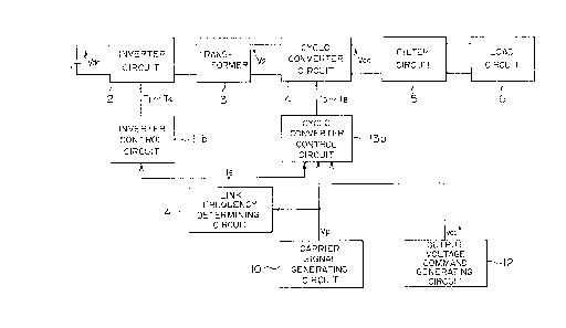
Fig. 10 is a block diagra~ which illustrates a power
conversion apparatus disclosed in~ for example, Japanese
Patent Application Wo. 1-211737. Referring to Fig. 10,
reference numeral 1 represents a DC power source, 2
represents an inverter circuit and 3 represents a
transformer the input terminal o~ which is connected to the
inverter circui~ 2.:: Reference numeral 4 represents a cyclo
converter circuî~ connected to the output terminal of the
transformer 3. Reference numeral 5 represents a filter
circuit connected to the output terminal of the cyclo
converter circuit 4. Reference numeral 6 represents a load
circuit connected to the output terminal of the filter
circuit 5. Reference numeral 10 represents a carrier
signal generating circuit, lla xepresents an inverter
control circuit, 12 represents an output voltage command
generating circuit for processing a command of an output
-2- 2~2~
voltage or an output current t~ansmitted from the cyclo
converter 4 and 13a represents a cycle converter control
circuit.
Fig 11 illustrates the detailed struc~ures of the
inverter circuit 2, the transformex 3 and the cyclo
converte~ circuit 4. The invert r circuît ~ comprises
semiconductor switching devices S1 to Sq composed of
transistors, MOSFETs or the like and diodes Dl to Ds which
are respectively, in an anti-parallel manner, connected to
the corresponding semiconductor switching devices Sl to S4.
The transformer 3 has a primary coil ~hich is connected to
the inverter circuit 2 and as well has a secondary coil
which is connected to the cyclo converter circuit 9. The
cyclo converter circuit 4 comprises semiconductor switching
devices S5 to S~ and S5A to 58A composed of transistors,
MOSFETs or the like and diodes Ds to D~ and DSA to D8A which
are respectively, in an anti-parallel manner, connected to
the corresponding switching devices S5 to S8 and S5A to S8A.
The two semiconductor swi.tching devices Sn and SnA (n = 5 to
8) and two diodes Dn and DnA (n = 5 to 8) connected to the
same in the anti-parallel manner constitute a bidirectional
switch Qn which is capable of controlling the power supply
direction.
As shown in Fig. 12, the inverter control circuit lla
comprises a 1/2 divider 100 which transmi~s an output
, , , . .. ..,
:: .: : :: . . . : . :: : ~ ,,
.. : - :- , ;: -, ~, . ..
- , , ,
3 2 ~ ~ rJ $ ~ ~
signal, the polarity of which is inverted in
synchronization with the last transition of an input
signal, and a NOT circuit 101 connected to the 1/2 divider
100. The inverter control circuit lla transmits drive
signals T1 to T4 to the inverter circuit 2, the switching
signals T1 to T4 being signals for switching on/off the
switching devices S1 to S4 of the inverter circuit 2.
Fig. 13 illustrates the detailed structure o~ the
cyclo converter con~rol circuit 13a which comprises an
absolute value circuit 102, a comparator 103, NOT circuits
105, 106, 108 and 110, 1/2 dividing circuits 104 and 107, a
polarity discriminating circuit 109, AND circuits 111 to
118 and OR circuits 119 to 122. The cyclo converter
control circuit 13a transmits dri~e signals T~ to Ts which
are signals for s~itching on/off switches Qs to Qs of the
cyclo converter circuit 9.
Then, the operation o~ the above-described
conventional apparatus will now be described with reference
to a timing chart shown in Fig. 19. First, a sawtooth
shape carrier signal Vp facing an upper right direction is
transmitted from the carrier signal generating circuit 10.
Then, drive signals T1 to T4, the duty ratio of each of
which is 50~, are, due to the following operations,
transmitted from the inverter control circuit lla shown in
Fig. 12: when the carrier signal Vp is supplied, signal
-
Tx, which synchronizes with the signal Vp and which is
halved, is transmitted from the 1/2 divider 100.
Furthermore, the NOT circuit 101 transmits signal Ty which
is a signal obtainable by inverting the sign of the signal
Tx. As a result, the signal Tx is, as the drive signals T
and T4, transmitted to the inverter circuit 2.
Furthermore, the signal Ty is, as the drive signals T2 and
T3, transmitted to the same. When the level of each of the
drive signals T1 to T4 is high, the corresponding switching
devices S1 to S4 of the inverter circuit 2 are switched on,
while the same are switched off when the above-described
level is low. Furthermore, the relationship between the
switching on~off operations of the semiconductor switching
devices Sl to S4 and the secondary voltage V2 of the
transformer 3 shown in Fig. 11 can be expressed as follows:
When the switches S1 and S~ are switched on: V2 = Vdc
When the switches S2 and S3 are switched on: V2 = - Vdc
... (1)
.where symbol Vdc denotes the output voltage from the DC
power source 1
Therefore, the secondary voltage V2 becomes a
rectangular wave voltage the duty ratio of which is 50% as
shown in Fig. 1~.
. .- ., .. ~ . ,
, :, . . : : - :
: . - ::: . . . .
. . . ...
-5-
On the other hand, the output voltage command
generating circuit 12 transmits output voltage command
signal Vcc* which instructs the output voltage to be
transmitted from the cyclo converter 4~ the output voltage
command signal Vcc* being, together with the carrier signal
Vp, supplied to the cyclo converter control circuit 13a.
The cyclo converter control circuit 13a receives the above-
described si~nals so as to transmit the drive signals Ts to
T~ the pulse width of each which has been modulated as
follows. Referring to Fig. 13, the output voltage command
signal Vcc* is converted into a~solute signal IVcc*l by the
absolute value circult 102. The absolute signal IVcc*l is,
together with the carrier signal Vp, supplied to the ~:
comparator 103. ~The comparator 103 transmlts signal Tp
shown in Fig. 14, the signal Tp being then supplied to the
1/2 divider 104 in which-the signal Tp is ~onverted into
signal Ta. On the other hand, when the signal Tp is
supplied to the 1/2 divider 107 after the sign of it has
been lnverted by the NOT circuit 105, signal Tb formed into
the same wave shape as that of the signal Tx is
transmit~edO Furthermore, when the signal Ta is supplied
to the NOT circuit 105, signal Tc is transmitted, while
when the signal Tb iS supplied to the NOT circuit 108,
signal Td formed into the same wave shape as that of the
signal Ty is transmitted.
' -6~
Then, the relationship between ~he signals Ta to Td and
output voltage Vcc from the cycle converter circuit 4 will
now be described. In a case where there is a desire to
make the polarity of the output voltage Vcc to be positive,
the drive signals Ts to Ta are determined in accordance with
the following equations:
T5 = Ta~ T6 = Td~ T7 = Tc~ T8 c Tb ., . (2~
In response to the above-described drive signals Ts to
Ta, the switch Qn (n = 5 to 8) which constitutes the
bidirectional switch is switched on/of~. As a result, the
output voltage Vcc f~om the cyclo converter circuit 4 is
controlled. The fact that the switch Qn iS switched on/off
means a fact that the switching devices Sn and SnA are
simultaneously switched on/off. The relationship between
the swltching on/off operation performed by the switch Qn
(n = 5 to 8) and the above~described output voltage Vcc is
expressed by the following equations:
When switches Qs and Qs are switched on: Vcc = V2
When switches Q6 and Q7 are switched on: Vcc = -- V2
...(3)
When switches Q5 and Q6 are switched on: Vcc = O
When switches Q7 and Q8 are switched on: Vcc = O
- ~,~": . .
.
'~ 2 ~ S~ ~
Therefore, the following facts can be deduced from
Equations (2) and (3): when the levels o~ ea~h of the
signals Ta and Tb iS high in Fig. 14, the relationship Vcc =
V2 is held, when the levels of each o~ the signals Tc and Td
i~ high/ the relationship Vcc = - V2 is held. When the
levels of each o~ the signals Ta and Td or the signals Tb
and Tc are high, the relationship Vcc = 0 is held.
Therefore, the output voltage Vcc from the cyclo converter
circuit 4, as shown in Fig. 14, becomes positive voltage
the pulse width of which has been modulated. In a case
where there is a desire to make the polarity of the output
voltage Vcc to be negative, the drive signals Ts to Ts may
be determined in accordance with the followlng equations:
Ts = Tc, T6 ~ Tb, T7 = Ta, T8 = Td . . . (4)
Then, the description about the operation shown in
Fig. 13 will now be continued. The polarity discriminating
circuit 109 transmits polarity signal Vsgn denoting the
polarity of the output voltage command signal Vcc*. The NOT
circuit 110 transmits a signal which is a signal obtainable
by inverting the sign of the polarity signal Vs~n . The
above-described signals and the signals Ta to Td are, via
the AND circuits 111 to 118, supplied to the OR circuits
119 to 122. When the polarity of the output voltage
-8- C~
command signal Vcc* is positive, the si.gnals Tat Tc, Td and
Tb are transmitted from the A~D circuits 111, 114, 116 and
117, respectively. Therefore, the drive signals Ts to T8 in
accordance with Equation ~2) are transmitted to the
switches ~5 to Qs of the cyclo converter circuit 4.
Similarly, when the polarity of the output voltage co~mand
signal Vcc* is negative, the drive signals Ts to Ts in
accordance wi~h Equation (4) are transmitted to the
switches Qs to Qs. As a result of the above-described
operations, the voltage Vcc, the wave form of which is
obtainable by modulating the pulse width of the AC output
voltage command signal Vcc* transmitted from the output
~oltage command generating circuit 12, is transmitted from
the cyclo converter circuit 4. In this state, the PWM
operation can be performed similarly by a method arranged
in such a manner that the output current transmitted from
the cyclo converter circuit 4 is detected and the switch Qn
~n = 5 to 8) of the cyclo converter circuit 4 is switched
in a single direction in accordance with the polarity of
the output current as follows:
when the polarity of the electric current is positive:
S5 = Ts, S6 = T6, S7 = T7, S8 = T8 ... (5)
All of switches S5A to S8A are switched off
- . - .~ , . .
.
- : ;,. . : . ,: ,. .
-: , :., .. :: -
- ~
.. ::
:~
~ -9-
When the polarity of the electric current is negative:
All of switches S5 to S8 are switched off
S5A ~ T5, S6A = T6, S7A = T7, S8A = T8 . . . (6)
Furthermore, the output from the cyclo converter
circuit 4 is supplied to the ~oad circuit 6 after the hlgh
frequency component of the output voltage Vcc has been
removed by the fil~er circuit 5.
The conventlonal power convexsion apparatus has been
constituted as described above in such a manner that it
receives the DC power and temporarily converts it into a
high frequency AC so as to transmit AC power which
corresponds to the output voltage c~mm~n~ signal by using
the high frequency AC power. Si~ce high fre~uency electric
power is txansmitted/received via a transformer in a DC-AC
power conversion apparatus of the type described above, it
is usually called a "hi~h frequency intermediate link type
power conversion apparatus". Furthermore, the frequency of
th~ electric power which is caused to pass through the
transformer as descrlbed above is called a "link
frequency". By employing the above-described high
frequency intermediate link method, the frequency of the
electric power which passes through the insulating
transformer can be raised ko a level which is several tens
of times of the output frequency. Therefore, the size and
. ~ : ~ . , . ; . .
1 0
the weight of the transformer can be reduced. However, in
a case where the above-described me~hod is employed in a
large~capacity power conversion apparatus, the link
frequency must, in fact, be lowered in inverse proportion
to the capacity in order to overcome a problem taken place
in that it is very difficult to constitute a high frequency
and large capacity transformer. The conventional structure
constituted as shown in Fig. 10 is arranged in such a
manner that the link frequency and the PWM frequency is
made to be 1:2. Therefore, the conventional structure
encounters a problem in that the PWM frequency of the cyclo
converter is lowered in proportion to the link frequency
and thereby the controllability of the output voltage
waveform of the power converter deteriorates and as well as
the size of the filter circuit cannot be reduced.
SUMM~RY OF THE INVENTION
An object of the present invention is to provide a
power conversion apparatus capable of overcoming the above-
described conventional problems, preventing deterioration
in the controllability of the output voltage waveform and
eliminating a necessity of using a large-size filter
circuit.
A power conversion apparatus according to the present
invention comprises: a reference signal generating circuit
for genera-ting a reference signal which has a first
.~; .. . .;
~ ~ :. :: ..
.: ~ . . . :: . .: ,. :. .. .. .
frequency; a first power converter for converting D.C.
power into A.C. power which has the first frequency; a
transformer connecte~ to the first power converter; a
carrier signal generating circuit for generating a caxrier
signal which has a second frequency which is higher than
the first frequency; a second power converter having a
plurality of switching means and as well as converting the
output from the transformer into A.C. power which has the
second frequency; a command signal generating circuit for
generating a command signal for commanding the quantity of
the output from the second power converter; and a second
power-converter control circuit for generating a drive
signal for driving a plurality of the switching means of
the second power converter in such a mannex that the drive ~:
signal is generated in response to the reference signal
generated by the reference signal generating circuit and a
command si~nal generated by the command signal generating
circuit and as well as in synchronization with the carrier
signal generated by the carrier signal generating circuitO
BRIEF DESCRIPTION OF THE DRAWINGS
Fig. 1 is a block diagram which illustrates a first
embodiment of a power con~ersion apparatus according to the
present invention;
Fig. 2 is a circuit diagram which illustrates an
in~erter control circuit according to the first embodiment;
.
-~2
Fig. 3 is a block diagram which illustrates a cyclo
converter control circuit according to the first
embodiment;
Fig. 4 is a timing chart which illustrates the
operation to be performed according to the first
embodiment;
Fig, 5 is a block diagram which illustrates a second
embodiment of the power conversion apparatus according the
present invention;
Fig. 6 is a circuit diagram which illustrates a
transformer, a cyclo converter circuit and a filter circuit
according to a second embodiment; ~ -
Fig. 7 is a block diagram which illustrates a cyclo
converter control circuit according to the second
embodiment;
Fig. 8 is a timing chart which illustrates the
operation to be performed according to the second
embodim~nt;
Figs. 9A and 9B are timing charts which illustrate the
operations to be performed according to another embodiments
: .
of the pre~ent invention;
Fig. 10 is a block diagram which illustrates a
conventional power conversion apparatus
~ ~ .. : .:,.. . . , ,.,, :
-13~
Fig. 11 is a circuit diagram which illustrates an
inverter circuit, a transformer and a cyclo converter ~'
circuit according to the conventional structure;
Fig. 1~ is a block diagram which illustrates an
inverter control circuit according to the conventional
structure;
Fig. 13 is a block diagram which illustrates a cyclo
converter control circuit according to the conventional
structure; and :
Fig. 14 is a timing chart which illustrates the ~:
operation to be performed according ~o the conventional :
.:
structure.
DESCRIPTION OF THE PREFERRED EMBODIMENTS
Preferred embodiments of the present invention will
now be described with reference to the drawings.
As shown in Fig. 1, a po~er conversion apparatus
:according to a firgt embodiment of the present invention is
constituted in such a manner that the inverter control
circuit 11a and the cyclo converter control circuit 13a of
the conventional power conversion apparatus shown in Fig.
10 are respectively replaced by an inverter control circuit
llb and a cyclo converter control circuit 13b.
Furthermore, a link frequency determining circuit 14 is
disposed between the carrier signal generating circuit 10
and the inverte~ control circuit llb. The link frequency
- . : :, :
- :: : :
.
.: . ~ ;
-l4~
determining circuit 14 divides the carrier signal Vp
generated by the carrier signal generating circuit 10 to
transmit ob~ained signal Te to the inverter control circuit
llb and the cyclo converter control circuit 13b.
As shown in Fig. 2, the inverter control circuit llb
has a NOT circuit 123 for inverting the signal Te
transmitted from the link frequen&y determining circuit 14
so as to transmit switch signals Tl to Ts to the inverter
circuit 2. -
As shown in Fig. 3, the cyclo converter control
circuit 13b comprises an absolute value circuit 1~2, a
comparator 103r NOT circuits 105, 108, I10 and 201, a : .
polarity discrimlnating circuit 109, AND circuits 111 to
118, 202 and 203~and 0R circuits 119 to 122, the cyclo
converter controL circuit 13b thus-constituted transmitting
drive signals Ts to Ts. The above-described drive signals
Ts to Ts are supplied to corresponding switches Qs to Qs of
the cyclo converter circuit 4.
Then, the operation of the first embodiment will now
be described with reference to a timing chart shown in Fig.
4. First, a savtooth shape carrier signal Vp facing an
upper right direction is transmitted from the carrier
signal generating circuit 10 to the link frequency
determining circuit 14 and the cyclo converter control
circuit 13b. Then, ~he above-described carrier signal Vp
~,, -, , , ., -. : - :, ,
-15~
. . .
is divided to l~n by the link frequency determining circuit
14. Fig. ~ illustrates a case where the same is quartered.
There~ore, the description will, with reference to Fig. 4,
be made about a case in which the P~M frequency is four
times the link frequency. In synchroni~ation with the last
transition of the carrier signal Vp, the quartered signal Te
is transmitted from the above-described link fxequency
determining circuit 14. Th~n, inverted signal Tf of the
signal Te iS processed by the NOT circuit 123 of the
inverter control circuit llb. As a result, the signal Te
is, as the drive signals Tl and T4, transmitted to the
inverter circuit 2, while the signal Tf is~ as the drive
signals T2 and T3, transmitted to the inverter circuit 2.
When the level of each of the drive signals Tl to Ts is
high, the corresponding switching devices S1 to S4 Of the
inverter circuit 2 are switched on. When the same is low,
the above~described switching devices Sl to S4 are switched
off. The following relationship between the switching
on/off operation of the semiconductor switching devices S
to S4 and the secondary voltage V2 of the transformer 3 is
deduced from Fig. 11:
When S1 and S4 are switched on: V2 = Vdc
When S2 and S3 are switched on: V2 = - Vdc ... (7
;
where symbol Vdc denotes the output voltage from the DC
power source 1.
Therefore, the secondary voltage V2 becomes a
rectangular wave voltage the duty ratio of which is 50% and
the frequency of which is 1/4 times that of the carrier
signal Vp as shown in Fig. 4.
On the other hand, the output voltage command
generating circuit 12 transmits output voltage co
signal Vcc* which instructs the output voltage to be
transmitted from the cyclo converter cixcuit 4 for the
purpose of controlling the electric current or the voltage ~ -
of the load circuit 6, the output voltage command signal
Vcc* being, together w1th the carrier signal Vp and the
signal Te transmitted~from the link frequency determining
:
circuit 14, supplied to the cyclo converter control circuit
13b. The cyclo converter control circuit 13b receives the
above-described signals so as to transmit the drive signals
Ts to Ts the pulse width of each which has been modulated as
follows. Referring to Fig. 3, the output voltage command
signal Vcc* is, first, converted into absolute signal IVcc* I
by the absolute value circuit 102. The absolute signal
IVcc*l is, together with the carrier signal Vp, supplied to
the comparator 133. The comparator 103 transmits signal Tp
shown in Fig. 4. The signal Te transmitted from the link
-l7~ 2 ~ & ~
frequency determining circuit 14 is inverted by the NOT
circuit 201 so ~hat it is formed into signal Te. The
signal Tp is subjected to a process in wh.ich the AND from
the signal Te is calcula~ed so as to be conver~ed into
signal Tg. On the other hand, the signal Tp is subjected to
a process in which the AND from the signal Te is calculated
so as to be converted into signal Tj. That is, the ~ignal
Tp is distributed into the signal Tg and T~ in accordance
with the level of the signal Te. Furthermore, the signal Tg
is inverted by the NOT circuit 105 so that it is converted
into signal Th. The signal T-J is inverted by the NOT
circuit 108 so that it is converted into signal Tk.
Then, the relationship between the signals Tg, Th, T
and Tk and output voltage Vcc from the cycle converter
circui~ 4 will now he described. In a case where there is
a desire to make the polarity of the output voltage Vcc to
be positive, the drive signals Ts to Ts are determined in
accordance with the following equations:
T5 = Tg, T6 = T~, T7 = Th, TB = Tk . . . ~8)
In response to the above-described drive signals Ts to
Ts, the switch Qn (n = ~ to 8) which constitutes the
bidirectional switch is swi~ched on/off. As a result, the
outpu~ voltage Vcc from the cyclo converter circuit 4 is
controlled. The relationship between the switching onfoff
operation performed by the switch Qn (n = 5 to 8) and the
above-described output voltage Vcc is expressed by the
following equations:
When switches Q5 and Q8 are switched on: Vcc = V2
When switches Q6 and Q7 are switched on: Vcc = - V2
~- ~ (9)
When switches Q5 and Q6 are switched on: Vcc = O
When switches Q7 and Q8 are switched on: Vcc = O
Therefore, the following facts can be deduced from
Equations (8) and (9~: when the levels of each of the
signals Tg and Tk iS high in Fig. 4, the relationship Vcc =
V2 iS held, when the levels of each of the signals Th and T~
is high, the relationship Vcc = - V2 iS held. When the
levels of each of the signals Tg and Tj or the signals Th
and Tk are high, the relationship Vcc = O is held.
Therefore, the output voltage Vcc from the cyclo converter
circuit 4, as shown in Fig. 4, becomes positive voltage the
pulse width of which has been modulated. In a case where
there is a desire to make the polarity of the output
voltage Vcc to be negative, the drive signals Ts to Ts may
be determined in accordance with the following equations:
Ts = Th, T6 = Tk, T7 = Tg, TB = Tj ~-.(10)
Then, the description about the operation shown in
Fig. 3 will now be continued. The polarity discriminating
circuit 109 transmits polarity signal Vsgn denoting the
polarity of the output voltage oommand signal Vcc*. The NOT
circuit 110 transmits a signal which is a siynal obtainable
by inverting the sign of the polarity signal Vsqn. The
above-described signals and the signals Tg, Th~ T~ and Tk
are, via the AND circuits 111 to 118, supplied to the OR
circuits 119 to 1220 When the polarity of the output
voltage command signal Vcc* is positive, the signals T~, Th~
T~ and Tk are transmitted from the AND circuits 111, 114,
115 and 117, respectively. Therefore, the drive oignals in
accordance with Equation (8) are transmitted to the
switches Qs to Qs of the cyclo converter circuit 4.
Similarly, when the polarity of the reference voltage Vcc*
is negative, the drive signals in accordance with Equation
~10) are transmitted to the switches Qs to Qs.
As a result of the above-described operations, the
voltage Vcc, the wave form of which is obtainable by, with a
~: .
frequency which is four times that of the link frequency,
modulating the pulse width of the output voltage command
signal Vcc* transmitted from the output voltage command
generating ci~cuit 12, is transmitted from the cyclo
converter circuit 4. Therefore, it can be understood that
- , , , : . ~ : :
-20- ~ J ~
the waveform, the pulse width of which is modulated by a
frequency which is n times that of the link frequency, is
transmitted from the cyclo converter circuit 4 by dividing
the carrier signal by n in the link frequency generating
circuit 14. In this state, the PWM operation can be
performed similarly b~ a method arra~ged in such a manner
that the output current transmitted from the cyclo
converter circuit 4 is detected and the switch Qn ~n - 5 to
8) of the cyclo converter circuit 4 is switched in a single
direction in accordance with the polarity of the output
current as follows:
whe~ the polarity of the electric current is positive:
Ss = Ts, S6 = T6, S7 = T7, S8 = T8 ...(11
All of switches SSA to S8A are switched off
.
When the polarity of the electric current is negative:
All of switches S5 tO S8 are switched off
S5A = T5, S6A = T6, S7A = T7, S8A = T8 . . . ~12
:
Furthermore, the output from the cyclo converter
circuit 4 is supplied to the load circuit 6 after the high
f requency component of the output voltage Vcc has been
removed by the filter circuit 5.
-2l~
Then, a second embodiment of the present invention
will now be described with reference to Figs. 5 to 8. Fig.
5 is a block diagxam which illustrates a second embodiment
of the present invention. The second embodiment of the
present lnvention is constituted similarly to ~he first
embvdiment e~cept for a structure arranged in such a manner
that the cyclo converter circuit 4c, the filter circuit 5c,
the output ~oltage command generating circuit 12c and the
cyclo converter control circuit 13c are respectively made
to be three-phase circuits.
Fig. 6 illustrates the detailed structure of the
transformer 3, the cycle converter circuit 4c and the
filter circuit 5c. The cyclo converter circuit 4c
comprises semiconductor switching devices such as
transistors or MG~SFETs as follows i~ order to transmit
three-phase voltage. A U-phase circuit is composed of
semiconductor swi~ching devices SU1, SU2~ SU1A and SU~A. A
pair composed of the switching devices Sul and SU1A and
another pair composed of the switching devices SU2 and SU2A
respectively constitute bidirectional switches Qun ~n = 1 to
2) with which the power supply direction can be controlled.
Also V and W phase circuits are respectively composed of
switches Qvn and ~wn with which the bidirectional control
can be performed. The filter circuit 5c which receives the
output from the cyclo converter circuit 4c is composed of
::
-22- ~ c~
three AC reactors LF and three capacitors CF to form an AC
filter.
Fig. 7 illustxates the detailed structure of the cyclo
converter control circuit 13c. Refexring to Fig. 7,
reference numeral 123u represents a U-phase control
circuit, 123v represents a V-phase control circuit and 123w
represents a W~phase control circuit. The U-phase control
circuit 123u comprlses a comparator 124, a NOT circuit 125
and EX-OR tExclusive-OR~ circuits 126 and 127 so that it
receives output voltage command signal Vu* transmitted from
the output voltage command generating circuit 12c, the
carrier signal Vp and the output signal Te transmitted from
the link frequency determining circuit 14 and transmits U-
phase drive signal Tul and Tu2 of the cyclo converter
circuit 4c. The structure of each of the V-phase control
circuit 123v and the W-phase control circuit 123w is made
to be the same as the U-phase control circuit 123u. The V-
phase control circuit 123v and the W-phase control circuit
123w respectively receive the output voltage command
signals Vv* and Vw* to transmit drive signals Tvl~ Tv2~ Tw1
and Tw2 for switching the cyclo converter circuit 4c. The
drive signals Tun~ Tvn~ Twn (n = 1, 2) respectively
correspond to the switches Qun~ Qvn and Qwn (n = 1, 2) of the
cyclo converter circuit 4c.
-2~
Then, the operation of the second embodiment will now
be described with reference to a timing chart shown in Fig.
8. The inverter circuit 2 performs the same operation as
that according to the first embodiment to transmit the
inverter outpu~ voltage V2 shown in Fig. 8.
On the other hand, the cyclo converter circuit 4c
shown in Fig. 6 1s constltuted similarly to a conventional
three-phase inverter e~cept for the fact that the cyclo
converter circuit 4c has the switching devices which act in
a bidirectional manner. Therefore, the cyclo converter
circuit 4c is able to control the three phases
individually. Therefore, the description will be made
about the U-phase. First, the output voltage command
generating circuit 12c transmits three-phase output voltage
command signals Vu*, Vv* and Vw* which are, together with
the carrier signal Vp and the signal Te transmitted from the
link frequency determining circuit 14, then supplied to the
cyclo converter control circuit 13c. The cyclo converter
control circuit 13c receives the above-described signals to
transmit drive signals Tu1 and Tu2 the pulse width of each
of which has been modulated.
First, the output voltage command signal Vu* is,
together with the carrier signal Vp, supplied to the
comparator 124 so that signal TPA shown in Fig. 8 is
transmitted. Therefore, the pulse width WPA of the above-
: : .
,
-24~
described signal TPA ~hen its level i5 high is widened in
accordance ~ith the positive level of the output voltage
command signal Vu*. On the other hand, it is narrowed in
inverse proportion to the negative level. Then, the signal
TPA is supplied to the NOT circuit 125 so that inverted
signal Tq shown in Fig. 8 is transmitted.
Assuming that the middle point of the secondary coil
of the transformer 3 is an imaginary ground O as shown in
Fig. 6, the potential Vuo of point U with respect to the
above described imaginary ground O is controlled in
accordance with switching of~off operation of the swltch Qn
(n = 1, 2) as expressed by using the secondary voltage V2
of the transformer 3:
When Qu1 is switched on: Vuo = V2/2 ... (13)
When Quz is switched on: VuO = - V2/2
There~ore, by distributing the si~nals T~A and Tq to
the drive signals Tu1 and Tu2 by utilizing the relationship
shown in Equation (13), the U-phase voltage Vu which
corresponds to the U-phase output voltage command signal
Vu~ is obtained. Assuming that the high level pulse width
of the signal Tq is Wqt the following relationship can be
obtained.
:
--25--
$ ~
VU = [ (WPA -- Wq) / (WPA + Wq) ] ~ V2/2 . . . (14)
However, the output voltage V2 from the in~er~er
circuit 2 is a rectangular wave voltage which swings
between a positive value and a negative value in accordance
with the link frequency. Therefore, the following
switching operation must be performed in accordance with
the change in the polarity of the rectangular wave ~oltage:
When V2 is positive, Tul = TPA, TU2 = Tq ... (15)
When V2 is negative, TU1 = Tq, TU2 = TPA ... (16)
Then, the description about the operation of the
stxucture shown in Fig. 7 will be continued. The signal Te
is a drive~signal with whlGh the above-described output
voltage V2 can ~e obtained. When the level of V2 is a
positive value, the level of the si~n~l Te is high. The
above-described signal Te is supplied to the EX-OR circuits
126 and 127, while the signal Tq is supplied to the EX-OR
circuit 126. Furthermore, the signal TPA is supplied to the
EX-OR circuit 127. If the level of either of the two input
signals is high, the EX-OR circuit transmits a polarity
in~erted signal of another signal. If the same is low, the
EX-OR circuit transmits the polarity of the residual
.
-26- 6~ ~ 2~
signal. Therefore, by assigning output signals Tm and Tc
from the EX-OR circuits 126 and 127 to the drive signals Tul
and Tu2, the above-described Equation (14) can be met. As a
result of ~he above-described operation, the cyclo
converter circuit 4c, as shown in Fig. 8, transmits voltage
Vu, the waveform of which is obtained by pulse~width
modulating the output voltage command signal Vu*
transmitted from the output voltage command generating
circuit 12 by a frequency which~is four times the link
frequency. Therefore, it can be understood that the wave
which has been pulse-width modulated by a frequency which
is n times the link frequency can be transmitted from the
cyclo converter 4c by dividing the carrier signal by n in
the above-described link frequency generating circuit 14.
In this~state,: the PWM operation can be perfor~ed
similarly by a method arran~ed in such a manner that the :
output current transmitted from the cyclo converter circuit
4c is detected and the switch Qn (n = S to 8) of the cyclo
converter circuit 4c is switched in a single direction in
accordance with the polarity of the output current as
follows:
when the polarity of the electric current is positive:
SU1 = TU1, SU2 = TU2,
SU1A and SU2A are switched off ... (17)
-27- 2~2~
When the polarity of the electric current is negative:
switches Su1 and SU2 are switched off
SU1A = TU1, SU2A -- TU2 . . . ~18 )
Furthermore, the output from the cyclo converter
circuit 4c is supplied to the load circuit 6 after the high
frequency component of the output voltage Vu has been
removed by the filter circuit Sc.
The above-described first and second embodiments are
arranged in such a manner that the frequency of the
inverter synchronizes with the carrier frequency of the
cyclo converter while holding a relationship of even~number
times. However, as shown in Fig. 9A, in a case where the
above-described frequencies synchronize with each other
while holding a relationship of odd-number times or, as
shown in Fig. 9B, in a case where they do not synchroni~e
with each other, the conversion apparatus arranged in
accordance with the principle of the present invention can
be constituted though the structure of operation control
circuit is complicated slightly.
Furthermore, the present invention is not limited to
the sine wave conversion apparatus acting with a constant
frequency and constant voltage such as the uninterruptive
power supply apparatus. It can, of course, be applied to
-:: .,
- ::~ .
. ~ . ~ , , :
:: . : : : : :
' ' ' ~: '' i..,' ~;
-28
the VVVF acting with the variable frequency and variable
voltage and as well as applied to, ~or example, an active
filter which is a device which transmits an electric
current in place of the voltage. In this case, it is
necessary for the structure of the output voltage command
generating circuit to be constituted in such a manner that
it generates the output voltaqe command in accordance with
the output current cor0mand value and the feedback value of
the output current.
Although the rectangular wave inverter is employed as
the first AC power source, it may be replaced by a
conversion apparatus such as a cyclo converter which acts
in accordance with another principle. Furthermore, a sine
wave inverter may be employed as an alternative to the
rectangular inverter. In a case where the sine wave power
source is employed, the structure must be arranged, for
ex~mple, in such a manner that a cosine comparator which is
arranged to act in consideration of th~ waveform of the
power source is used in the control circuit. Therefore,
the conversion apparatus acting in accordance with the
principle of the present invention can, of course, be
constituted although the structure is complicated slightly.
,- : - :., . - . ~:. , ,