Note : Les descriptions sont présentées dans la langue officielle dans laquelle elles ont été soumises.
2 ~
TITLE OF THE INVENTION
VOLTAGE DETECTOR FOR PRODUCING OUTPUT SIGNAL WITHOUT
TRANSIENT ERROR LEVEL
FIELD OF TH~ INVE,NTION
This invention relates to a voltage detector and,
more particularly, to a voltage detector for monitoring a
power voltage ~evel to see whether or not the power voltage
level is decayed under a predetermined level.
DESCRIPTION OF THE RELATED ART
A typical example of the voltage detector is
illustrated in Fig. 1, and comprises a voltage comparator
1, a reference voltage producing circuit 2 for supplying a
reference voltage level Vref to the voltage comparator 1,
and a monitored voltage producing circuit 3 for supplying a
monitored voltage level Vm to the voltage comparator 1.
The reference voltage producing circuit 2 is implemented by
a series combination of a resistor R1 and a zener diode D1
coupled between a power voltage line 4 and a ground voltage
line GND, and the reference voltage level Vref is produced
at a reference node N1 between the resistor R1 and the
zener diode D1. The monitored voltage producing circuit 3
is implemented by a series combination of resistors R2 and
R3 coupled between the power voltage line ~ and the ground
voltage line GND, and the monitored voltage level Vm i5
~63.~22
produced at a monitored node N2 between the resistors R2
and R3. The voltage comparator 1 compares the monitored
voltage level Vm with the reference voltage Vref, and
supplies an output signal Sout at an output node OUT1. The
output signal Sout is indicative of the relation between
the xeference voltage level Vref and the monitored voltage
level Vm.
~ ssuming now that the power voltage line 4 gives rise
to increase a power voltage level Vp as shown in Fig. 2,
the re~erence voltage level Yref is increased together with
the power voltage level Vp, and the monitored volta~e
producing circuit 3 keeps the monitored voltage level Vm
lower than the power voltage level Vp. If the power
voltage level Vp exceeds a breakdown voltage level Vd at
time t2, the reference voltage producing circuit 2 fixes
the reference voltage level Vref to the breakdown voltage
level. The power voltage level Vp continues to be
increased with time, and the monitored voltage level Vm
exceeds the reference voltage level Vref at time t3. Then,
the output signal Sout is elevated from the ground voltage
level to the power voltage level Vp, and the power voltage
level Vp and the output signal Sout are increased together.
The reference voltage level Vref is kept at the breakdown
, ~
,:
~3a2~
voltage level Vd regardless of the power voltage level V~,
and the monitored voltage level Vm is also increased.
On the other hand, the power voltaqe line 4 gives
rise to decrease the power voltage level Vp at time t4, and
the monitored voltage level Vm fo:Llows the power voltage
level Vp. If the monitored voltage~ level Vm becomes lower
than the reference voltage level Vref or the breakdown
voltage level Vd at time t5, the output signal Sout is
rapidly decayed from the power voltage level Vp to the
ground voltage level. The power voltage level ~p reaches
the reference voltage level Yref or the breakdown voltage
level Yd at time t6, and the zener diode D1 does not allow
current to flow therethrough. Then, the reference voltage
level Vref is decayed together with the power voltage level
Vp, and all the voltage levels finally reach the ground
voltage level.
Thus, the voltage comparator 1 monitors the monitored
voltage level Vm and, accordingly, the power voltage level
Vp to see whether or not the power voltage level Vp is
available for an associated electric circuit without any
trouble.
However, a problem is encountered in the prior art
voltage detector in that the output signal Sout is
transiently changed from the ground level to a positive
2~fi3~22
voltage level as labeled with X1 and X2 in Fig. 2. This is
because of the fact that component transistors of the
voltage comparator 1 are unstable in the power voltage
level Vp close to the grvund voltage level GND.
S[~MMARY OF THE INVENTION
It is there~ore an important ob~ect of the present
invention to provide a voltage detector which is free from
transient voltage lift.
To accomplish the object, the present invention
proposes to forcibly fix an output signal to an inactive
level while component transistors are unstable.
In accordance with the present invention, there is
provided a voltage detector for monitoring a target voltage
level to see whether or not the target voltage signal
exceeds a predetermined voltage level, comprising: a) a
reference voltage producing circuit coupled between a first
voltage line for the target voltage signal and a second
voltage line substantially constant in voltage level, and
operative to produce a reference signal substantially
proportional in voltage level to the target voltage signal
while the target vol~age signal is lower than the reference
voltage level, the reference voltage signal being
substantially constant at the reference voltage level after
20~3~2
the target voltage siyna]. is approximately equal to or
higher than the reference voltage level, the reference
voltage level being proportional to the predetermined
voltage level; b) a monitored voltage level producing
circuit coupled between the first voltage line and the
second voltage line, and operative to produce a monitored
voltage signal substantially proportional in voltage level
to the target voltage signal, c) a voltage comparator
operative to compare the monitored voltage signal with the
reference voltage signal, and producing an output signal
indicative of whether or not the target voltage signal
exceeds the predetermined voltage level; and d) a
prohibiting means provided in association with the voltage
comparator, and operative to forcibly fix the output signal
to an inactive level while the voltage comparator is
unstable in operation.
BRIEF DESCRIPTION OF THE DRAWINGS
The feature and advantages of the voltage detector
according to the present invention will be more clearly
understood from the following description taken in
conjunction with the accompanying drawings in which:
Fig. 1 is a circuit diagram showing the arrangement
of the prior art voltage detector;
Fig. 2 is a graph showing the circuit behavior of the
3~2~
prior art voltage detector,
Fig. 3 is a circuit diagram showing the arrangement
of a voltage detector according to the present invention;
Fig. 4 is a graph showing the circuit behavior of the
voltage detector shown in Fig. 3; and
Fig. 5 is a circuit diagram ~showing khe arrangement
of another voltage detector according to the present
invention.
DESCRIPTION OF THE PREFERRED EMBODIMENTS
First Embodiment
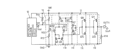
Referring Eirst to Fig. 3 of the drawings, a voltage
detector embodying the present invention largely comprises
a voltage comparator 11 coupled between a power voltage
line Vdd and a ground voltage line GND, a reference voltage
producing circuit 12 coupled between the power voltage line
Vdd and the ground voltage line GND and operative to
produce a reference voltage level Vref at a reference node
N11, and a monitored voltage producing circuit 13 coupled
between the power voltage line Vdd and the ground voltage
line GND and operative to produce a monitored voltage level
Vm proportional to a power voltage level Vp at a monitor
node N12.
Though not shown in detail, the reference voltage
' ' '' . ~ ,.
~;
,'
~3~2
producing circuit 12 is implemented by a p n-p band-gap
structure, because it is difficwlt for MOS technology to
produce a zener diode. While the power voltage level Vp is
lower than a critical level Vc inherent in the p-n-p band-
gap structure, the reference voltage producing circuit 12
gives rise to increase the reference voltage level Vref
together with the power voltage level Vp on the power
voltage line Vdd. However, after the power voltage level
Vp exceeds the critical level Vc, the reference voltage
producing circuit 12 keeps the reference node N11 in the
reference voltage level Vref in the critical level Vc.
The monitored voltage producing circuit 13 is
implemented by a series combination of resistors R11 and
R12, and the monitored voltage level Vm is given as
Vm = Vp x r12 / ~r11 + r12 ) ... ~quation 1
where r11 and r12 are resistances of the resistors R11 and
R12.
The voltage comparator 11 largely comprises an input
differential amplifier stage 11a, a constant current source
llb, an inverter stage 11c, and an output driver stage 11d.
The input differential amplifier stage 11a is implemented
by field effect transistors Q1 to Q4, and field effect
transistors Q5 to Q~ constitute the constant current souxce
11b. The inverter stage 11c is implemented by a series
2~6~2~
combination of field effect transistors Q9 and Q10, and the
output driver stage 11d is also implemented by a series
combination of field effect transistors Q11 and Q12. The
output driver stage 11d drives an output node OUT11, and an
output signal Sout takes place at the output node OUT11.
The voltage detector implementing the first
embodiment further comprises a clamping resistor R13 and a
clamping resistor R14, and the resistors R13 and R14 as a
whole constitute a prohibiting means. The clamping resistor
R13 is coupled between the power voltage line Vdd and the
reference node N11, and the clamping resistor R14 is
coupled between the output node OUT11 and the ground
voltage line GND.
Description is hereinbelow made on the circuit
~ehavior of the voltage detector with reference to Fig. 4,
and the voltage detector is assumed to invert the output
signal Sout upon voltage drop to 4.0 volts. The critical
level Vc is adjusted to 1.5 volts, and resistances r11 and
r12 are calculated from Equation 1. When the power voltage
le~el Vp reaches 4.0 volts, the monitored voltage level Vm
should be 1.5 volts. ~quation 1 is
1.5 = 4.0 x r12 / (rl1 ~ r12)
Therefore, r11 is (5/3)r12.
.
: ' '
2~3S2~
The power voltage line Vdd starts on increasing the
power voltage level Vp from the ground voltage level at
time t11, and reaches the critical level Vc at time tl2.
The reference voltage level Vref is fixed to the critical
level Vc. The output signal Sout remains in the ground
voltage level between time t11 and time tl2, and no error
level takes place. This is because of the ~act that the
reference node Vref is clamped to the power voltage level
Vp by means of the clamping resistor R13. However, the
monitored voltage level Vm is surely lower than the power
voltage level Vp, and the reference node N11 of the power
voltage level Vp prevents the voltage comparator 11 from
unstable state. In general, field e~fect transistors
become stable around the power voltage level Vp at about
2.0 volts, and the voltage comparator 11 never makes error
thereafter.
The power voltage level exceeds 4.0 volts at time
tl3, and the monitored voltage level Vm also exceeds the
critical level Vc. Then, the voltage comparator 11 inverts
the output signal Sout, and the output signal Sout is
elevated to a positive high voltage level slightly lower
than the power voltage level Vp due to the clamping
resistor R14.
The power voltage level Vp is decayed from time t14,
~3~2~
and the monitored voltage level Vm becomes lower than the
reference voltage level Vref at time t15. Then, the output
signal Sout is rapidly decayed to~ard the ground voltage
level, and undershoot US takes place. However, the output
signal Sout is quickly recover~d to the ground voltage
level, and is clamped at the ground voltage level by virtue
of the clamping resistor R14. The power voltage level Vp
reaches the critical level Vc at time t16, and the
reference voltage level Vref is decreased together with the
power voltage level Vp. However, the output signal Sout is
still clamped at the ground voltage level, and any error
level does not take place.
As will be appreciated from the forgoing description,
while the power voltage level Vp is too low to make the
component field effect transistors Q1 to Q12 of the voltage
comparator 11 stable, the clamping resistors R13 and R14
prevent the output signal Sout from error level, a~d the
voltage detector according to the present lnvention is
reliable.
Second Embodiment
Turning to Fig. 5 o~ the drawings, another voltage
detector embodying the present invention is illustrated.
The voltage detector implementing the second embodiment is
1 0
2~3~22
similar in circuit arrangemenk to the first embodiment
except for prohibiting means, and circuit components are
labeled with the same references used in ~ig. 3 without any
detailed description.
The prohibiting means of the second embodiment is
implemented by three clamping resistors R21, R22 and R23.
The clamping xesistor R21 is coupled between the power
voltage line Vdd and the reference node N11, and is
corresponding to the clam~ing resistor R13. The clamping
resistor R~2 is coupled between the output node OUT11 and
the ground voltage line GND, and is corresponding to the
clamping resistor R1~. The clamping resistor R23 is newly
added between the power voltage line Vdd and the input node
N21 of the output driver stage 11d, and the clampin~
resistor R23 makes the output signal Sout stable. In
detail, the inverter stage 11c and the output driver stage
11d are assumed to respectively have the minimum
operational voltage levels Vmin1 and Vmin2, and the output
signal Sout becomes unstable if Vmin1 is larger than Vmin2.
However, the clampiny resistor R23 pulls up the input node
N21, and causes the inverter stage 11c and the output
driver stage 11d to be stable. Therefore, the output
signal Sout is much more reliable even if the power voltage
level Vp is too low to make the component field e~fect
1 1
2~3~
transistors Q1 to Q12 stable.
Although particular embod.iments of the present
invention have been shown and described, it will be obvious
to those skilled in the art that various changes and
modifications may be m~de without departing from the spixit
and scope of the present invention.