Note : Les descriptions sont présentées dans la langue officielle dans laquelle elles ont été soumises.
2~6379~
WO 91tO157~ PCI/US90/03515
,. . .~
.~,, , .. ,. ;. .
MULTI-RESONANT LAMINAR ANTENNA
Technica~ E~
This invention relates generally to antennas, and more .
specifically to micro-strip antennas.
Back~round Art
For portable communication devices such as two-way
radios and pagers, the current trend in radio design is towards
20 product miniaturization. One of the largest components in the
radio, is the antenna. To reduce the antenna size, one solution is
to use conventional micro-strip antennas, where the resonators
are printed on a substrate using conventional thick or thin film
processlng.
Another trend in radio design is to use one broad-band
antenna for multi-frequency operation. Since one antenna would
eliminate the inconvenience of storing multiple parts, a low-profile
broadband antenna is desired~ However, micro-strip antennas
(resonators) are inherently narrow band. To broaden a single
30 microstrip antenna, one solution has been to stack a set of
microstrip antennas of differant resonant frequencies on top of
each other. In this way, the resonant frequencies of each antenna
combine to simulate a broadband frequency response.
Unfortunately, stacked antennas along with the associated
35 matching network increase the thickness of the antenna. In many
.
. . . . . .
~, ,
. .
WO 91/01~77 PCr/US90/03515
2~379~ ~
radios there is less room for a thickness increase than a width
increase.
In addition, exciting multiple resonators requires multiple
individual feeds. Often, the feed is accomplished by a feed probe
5 that protrudes through a dielectric layer. For manufacturing
simplicity, drilling through dielectric layer is not favored.
Therefore, a low-profile broadband antenna with a single external
feed is desired.
10 Summary of the Inventi~n
Accordingly, it is an object of the present invention to
provide a low-profile broadband antenna with integral matching
and a single external feed.
Briefly, according to the invention, a multi-resonant
15 antenna comprises a plurality of resonators which resonate at
different frequencies. A feed member is coupled to the multiplicity
of resonators. Disposed between and separating the resonators
from the feed member is a dielectric substrate.
20 Brief Descrlption of the Drawings
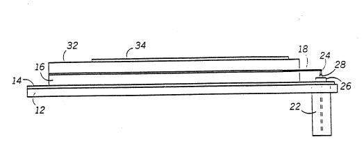
Figure 1 is a side-view of an antenna in accordance with ~-~
the present invention.
Figure 2 is a top view of the antenna of Figure 1.
Figure 3 is a side-view of an alternate embodiment of an
2~ antenna in accordance with the present invention.
Figure 4 is a top viaw of the antenna of Figure 3.
Figure ~ is a side-view of another alternate embodiment of
an antenna in accordance with the present invention.
Figure 6 is a top view of the antenna of Figure 5.
Detaile~ on of the Preferred Embodiment
Referring to Figure 1, the assembly of an antenna in
accordance with the present invention is shown. Using common
thick or thin film processing, metal is deposited on top of a
` 35 substrate 12 to form a ground plane 14. The material of the
substrate 12 may be ceramic or be formed from any other suitable
,.
,
' . "~' " ' :'
,
WO 91/01577 2 ~ 6 3 7 9 ~ PCr/US90/03515
, ' J ~
material. Located on top of the ground plane 14 is a layer of
dielectric material 16. A thin feed member 18 is placed on top
and extends beyond a portion of the dielectric layer 16 for
attachment to a 50 ohm connector 22 via a center conducting
5 feed line 24. The ground 26 of the conductor 22 is suitably
connected to the ground plane 14. As is common in 50 ohm
connectors, an insulator 28 insulates the center feed line from
ground. As illustrated, the 50 ohm conn~ctor 22 is located
external to the dielectric material 16 for ease of assembly (to not
10 have to drill through the dielectric material).
A top layer of dielectric material 32 is located on top of the
feed member 18 and the rest of the uncovered bottom dielectric
layer 16. The two layers of dielectric material may be bonded
together with a conventional thick or thin film agent or
1 5 sandwiched together by other suitable means. hnally, a metal
pattern 34 is deposited or laminated (formed such as by
conventional thin-film photo-imaging process) atop the top
dielectric layer 32 and overlays a portion of the fesd member 18.
Referring to Figure 2, the metal pattern 34 comprises a
20 plurality of substantially rectangular strips 34', 34" and 34"' which
are of different lengths to resonate at different frequencies as
determined by the air above and the dielectric material 32 below.
However, by using a different dielectric material below each
resonator, the resonating strips can be made (laminated) to be of
25 the same lengths and still resonate at different frequencies to form
similar resonators.
The tapered polygonal feed member 18 excites the
resonating strips 34', 34" and 34"' by capacitive coupling. The
length of the feed member 18 at its roctangular end being
30 overlayed by the top resonators 34 and the distance between the
feed member 18 and the resonating strips 34', 34", and 34"'
provide the proper matching for the antenna at the ~0 ohm
connector input 22. For optimum capacitive coupling, the thinner
the layer of resonating strips 34', 34n, and 34n', the less overlap is
35 needed. In this way, the excitation of multiple resonators 34', 34",
and 34"' is accomplished with one external feed 22.
.- . - . ~. ~ ~ .
: , . ,
~, , .
WO 91/01577 PCr/US90/03515
~3~
Referring to Figure 3, an alternate embodiment of the
present invention is shown to excite the resonators of different
polarizations using the same concepts. A 50 ohm connector 222
(the same connector 22 is shown simplified from hereon) is
attached to the center of a substrate 212. As before, a metal
pattern 234 is d~posited on top of a top dielectric layer 232 which
covers a portion of a feed member 218 which is atop a bottom
dielectric layer 214. The bottom dielectric laysr is located on top
of a ground plane 214 which is deposited on top of the substrate
212.
Referring to Figure 4, a top view of the alternate
embodiment of Figure 3 is shown. The feed mamber 218 is
circular in this embodiment to accommodatè the multi-resonating
strips 234' and 234r of one polarization and 234"'and 234"" of the
1 5 orthogenel polarization, which are radially disposed relative to `
the feed membQr 218. Again, the excitation of multiple resonators
234' 234", 234'n, and 234"n, is accomplished by a single feed 222
which does not protrude through the dielectric layers 232 and
214.
Referring to Figure 5, another alternate embodiment of the
antenna in accordance with the present invention is shown. As
before, metal is deposited on top of a substrate 312 to form a
ground plane 314. Located on top of the ground plane 314, is a
layer of dielectric material 316. A feed member 31 8 is placed on
top and extends beyond a portion of the dielectric layer 316 for
attachment to a 50 ohm connector 322 via a center conducting
feed line 324. As illustrated, the 50 ohm connector 322 is located
extemal to the dielectric material 316.
A metal pattem 334 is also deposited or laminated atop the
dielectric layer 316 and is capacitively coupled (not physically
connected) to the feed member 318.
Referring to Figure 6, the metal pattern 334 comprises a
plurality of substantially rectangular strips 334', 334" and 334"'
~, which are of different lengths to resonate at different frequencies
35 as determined by the air above and tha dielectric material 316
below.
., , . . ;
:
.
,:. ' . ` ' . ' , ~ . ' ' '
t WO 91/01577 2 0 6 3 7 9 ~ PCr/US90/03S15
The tapered polygonal feed member 318 excites the
resonating strips 334, 334n~ and 334n~ by capacitive coupling.
The distance between the feed member 318 and the resonating
strips 34, 34n~ and 34nl help provids the proper matching for the
5 antenna at the 50 ohm connector input 322~ For optimum
capacitive coupling, the widsr the resonating strips 34~ 341~ and
34~ ths less spacing is needed between the feed member 318
and the strips~ In this way, the excitation of multiple resonators
334., 334n~ and 334~ is accomplished with one sxternal feed 322.
What is claimed is:
,
, . .,, .: . ,: :
- . . .
- . . . . .
,, ' ' ' . ~ . ' :
,