Note : Les descriptions sont présentées dans la langue officielle dans laquelle elles ont été soumises.
CA 02064922 1998-03-12
'.~,~
TAPERING SIDEWA~LS OF VIA HOLES
FIELD OF THE INVENTION
This invention relates to a method of tapering
sidewalls of via holes for an integrated circuit and a via
hole structure for an integrated circuit.
BACKGROUND OF THE INVENTION
In fabrication of CMOS devices for V1SI integrated
circuits, conductive paths or contacts between first and
second conductive films separated by a intervening
dielectric layer are formed by defining a via hole or
contact hole through the dielectric layer, and then filling
the via with conductive material. For example, a
dielectric layer of an insulating material such as silicon
dioxide, is deposited on a first conductive layer
comprising a metal or alloy, such as sputtered aluminium.
The insulating layer is selectively masked, and a contact
hole or via hole is etched through an exposed region in the
insulating layer to expose the underlying conductive layer.
A second conductive layer, e.g. sputtered aluminium, is
deposited over the insulating layer, with conductive
material extending into the via hole, thereby forming a
contact between the two conductive layers. Alternatively
the via hole may be filled with a plug of conductive
material before deposition of the second conductive layer.
Integrated circuits incorporating multilayer
conductors may comprise three or more conductive metal
layers, each defining metal lines, and separated from the
other metal layers by intermetal dielectric layers. In a
triple level metal (TLM) structure having three layers of
metallization, contact via holes from a first conductive
layer to second conductive layer and then from second to
third conductive layer, must each pass through at least one
layer of intermetal dielectric. To provide a planarized
structure having a relatively smooth surface topography,
via holes having a depth differential of 25000A may be
required between the different levels of conductive layers.
The critical ~im~nsions or "cds" of the via hole,
~ I?
CA 02064922 l998-03-l2
that is, the maximum and minimum diameter of the contact
area with a conductive layer, are controlled so as to
comply with the design rules for semiconductor device
structures. In particular, the area defined by the bottom
diameter of a via hole should lie within the line width of
conductive metal lines. The via hole diameter should
provide for sufficient contact area for satisfactory
electrical performance, but overlap into other regions
which may cause electrical problems should be avoided. To
simplify the layout of an integrated circuit, it is
preferable that deep and shallow via holes are provided
with the same critical ~;men~ions.
Further, in order to provide reliable electrical
contacts, it is important that the deposited metal
satisfactorily fills the via hole, i.e. provides adequate
"step coverage" over the sidewalls, base and edges of the
hole without leaving voids or non-uniform regions. It is
well known that step coverage of sputtered metal in a deep
via hole is improved by tapering of the sidewalls of the
via hole, so that the diameter of the via hole is greater
at the top than at the bottom. Sidewall tapering of via
holes is particularly desirable to obtain adequate step
coverage of sputtered metal in via holes having high aspect
ratios, i.e. where the depth to width ratio is greater than
0.5.
A number of approaches to tapering sidewalls of via
holes of uniform depth are known. Generally dry etching
methods based on known isotropic and anisotropic reactive
ion etch processes which avoid or m;n;m;ze surface damage
are preferred for defining structures of small geometry.
More aggressive etch processes, including sputter etching,
are avoided and generally considered unsuitable for
defining submicron features such as via holes.
One approach is to provide for a progressive change
in etch rate during the process of etching a via hole. For
example, an insulating film may be deposited wherein the
composition of the insulating film changes with thickness
CA 02064922 1998-03-12
to provide a gradient in etch rate: German Patent DE3914602
discloses deposition of the insulating film as three
separate thin layers of different composition and Japanese
Patent J56131948 discloses method of depositing an
insulating glass layer having a composition gradient. Both
these structures provide for a differential etch rate
through the thickness of the insulating layer. Another
approach is to provide an insulating film of homogeneous
composition and to change the etchant composition
lo progressively as etching proceeds, for example, during a
reactive ion etching process, by successively changing the
composition of reactive gases in stages as the etch process
proceeds. As an example, in U.S. Patent 4,814,041 to Auda
there is disclosed a process wherein the composition of
plasma etchant is changed to provide an increased
concentration of oxidizer as etching proceeds. U.S. Patent
4,985,374 to Tsuji discloses use of successive dry etching
steps to form a stepwise tapered contact hole and U.S.
Patent 4,986,877 to Tachi discloses a temperature gradient
during etching to control etch rate as a function of etch
depth. However, it will be appreciated that problems arise
in such complex multistage processing in maintaining
precise control of the etching process to provide via holes
of a uniform depth while maintaining cds, and it will be
apparent that etching of via holes of large depth
differential is impractical by the above-mentioned methods.
Another known method of tapering sidewalls of via
holes, e.g. as described in U.S. Patent 4,948,743 to
Matsushita, includes providing a dielectric layer which may
be heated and caused to reflow around a via hole, thereby
rounding off the edges and tending to taper the via hole.
Any dielectric which tends to flow into the base of the
hole and cover the conductive layer is then removed by
reactive ion etching. However, this method has the
disadvantage that the resulting sidewall taper is small,
and the contact area is not reliably defined by a
lithographic step, but depends on the extent and uniformity
~3
CA 02064922 1998-03-12
'_
of the reflow step.
In yet another approach, a tapered sidewall spacer
is formed within a steep-sided via hole, by deposition of a
film of silicon dioxide or polysilicon which is then
anisotropically etched to leave a rounded sidewall spacer
having a tapered upper edge, so that the tapered sidewall
defines a smaller area contact hole, self-aligned within
the original steep-sided hole, as disclosed in U.S. Patent
4,489,481 to Jones and Japanese patent J01273333 to Natori.
o This technique provides a small taper to the top part of
the sidewall, while the bottom part is vertical due to the
anisotropy of the reactive ion etching process. To
increase the taper, the thickness of deposited oxide has to
be increased to more than 5000~ and consequently requires
etching of a correspondingly oversized steep-sided via hole
to allow for the thick sidewall spacer. This results in
the disadvantage that the m;n;mllm metal line width must be
large enough to accommodate the oversized steep-sided hole.
Furthermore, since the sidewalls define a self-aligned
contact area within the steep-sided hole, the bottom
diameter of resulting tapered via hole is not directly
defined lithographically.
With the exception of the latter method,
application of the above-mentioned methods of sidewall
tapering to tapering of via holes of different depth,
particularly for via holes of large depth differential,
would require that shallow via holes and deep via holes be
defined in separate sequences of process steps. However,
since each sequence itself involves multiple process steps,
the above-mentioned methods are impractical and
unsatisfactory for etching via holes for multilevel
interconnect structures. Consequently, other approaches
have been developed for simultaneously etching via holes of
different depths for multilevel metal interconnects.
For example, one known method provides for a
shallow isotropic etch to provide a tapered tbowl-shaped)
shallow portion and then an anisotropic etch from the
~,
~ :b
CA 02064922 1998-03-12
~,_
centre region of the shallow portion of the via hole so as
to create a steep-sided, deep portion (i.e. the via hole is
shaped like a countersunk screw hole). The metal layer at
the bottom of the shallow via holes acts as an etch stop
during further etching of the deep via holes down to the
deeper level metal. Shallow via holes are pre~o~in~ntly
tapered and bowl shaped, with a short, steep-sided deeper
portion; deep via holes comprise a corresponding shallow
tapered portion plus a deeper steep-sided portion, but
lo consequently the deeper via holes are difficult to fill
with sputtered metal of good quality. Although the
diameter at the base of the via holes is controlled by the
anisotropic etch (i.e. defined by masking/lithography), the
isotropic etch depth cannot be deeper than the shallowest
via holes without losing the cd of the shallow via holes.
Thus, for example, where the depth differential between
shallow and deep via holes is ~5000A, and the via hole size
is less than 1.5 to 2.0~m, this latter method is not
satisfactory.
Another known method for sidewall tapering of
multiple depth via holes is based on a multi-step resist
erosion process, which creates a via hole having stepped
sidewalls. The process involves defining openings in a
thick film of resist and anisotropically etching a via hole
partially through an insulating film to a first
predetermined depth. Then edges of the resist are eroded,
for example, by an isotropic etch or sputtering processes
to enlarge the hole in the mask, followed by a further
anisotropic etch to enlarge the top part of the via hole
and cut deeper into the previously etched first centre
portion of the via hole, resulting in a step in the
sidewall. The process steps of resist erosion and
anisotropic etching are repeated until each via hole
reaches the required depth and the underlying metaI
provides an etch stop. In this way via holes of differing
depths having staircase-like stepped sidewalls may be
created. However, the cd (bottom diameter) of shallow via
CA 02064922 1998-03-12
holes is greater than deep via holes, this difference being
significant when the depth differential between shallow and
deep via holes is high. Furthermore, the process re~uires
an initial undesirably thick coating of resist followed by
multiple process steps and the resulting stepped profile
may not provide for satisfactory step coverage.
SUMMARY OF THE INVENTION
The present invention seeks to provide a via hole
structure and a method of tapering sidewalls of via holes
for integrated circuits which avoids or reduces the above-
mentioned problems.
According to one aspect of the present invention,
there is provided a method of tapering sidewalls of via
holes comprising: providing a substrate having a
conductive layer, an insulating layer overlying the
conductive layer, the insulating layer defining
therethrough a steep-sided via hole, the insulating layer
forming a steep sidewall of the via hole extending from a
peripheral edge to a bottom of the hole and the underlying
conductive layer being exposed at the bottom of the via
hole; providing a protective layer of a uniform
predetermined thickness extending over the insulating layer
and over sidewalls of the via hole and over the exposed
conductive layer within the via hole; and sputter etching
the protective layer and the insulating layer to remove the
protective layer and etch the insulating layer, whereby
during sputter etching to remove the uniform predetermined
thickness of the protective layer from the conductive
layer, material of the insulating layer is removed by
sputtering from the peripheral edge and from the sidewall
of the via hole thereby smoothly tapering the sidewall, to
provide a tapered via hole increasing continuously in
diameter from the bottom of the via hole towards the
peripheral edge of the via hole.
Thus via holes having smoothly tapered sidewalls
are provided using a single sputter etching step. Problems
associated with surface damage caused during sputter
CA 02064922 1998-03-12
etching are avoided by providing a protective layer over
the conductive layer in the via hole. Preferably, where an
electrical contact is to be made to the underlying
conductive layer within a via hole, any sputtered debris
remaining in the via hole after the sputter etch step is
removed, for example by reactive ion etching to expose the
conductive layer. Thus a conductive layer having a clean
surface free of sputtered material is provided so that
reliable electrical contacts may be formed.
o Preferably the protective layer is a layer of the
same material as the insulating layer, and the protective
layer is provided by chemical vapour deposition.
Advantageously, the steep sided via holes are cleaned with
photoresist stripper before deposition of the protective
layer. Where the insulating layer and the protective layer
are silicon dioxide, the sputter etch preferably comprises
an argon sputter etch and any sputtered material remaining
in the via hole after sputter etching may be removed
conveniently from the via hole by reactive ion etching.
Thus, a smoothly and uniformly tapered via hole of an
arbitrary depth is produced in a reduced number of process
steps.
According to yet another aspect of the present
invention there is provided a method of tapering sidewalls
of via holes for multilevel interconnect structures,
comprising: providing a substrate having a conductive
layer and an overlying insulating layer, the insulating
layer defining steep sidewalls of a plurality of deep and
shallow via holes extending therethrough, a shallow via
hole extending through a first thickness of the dielectric
layer and a deep via hole extending through a second and
greater thickness of the insulating layer, portions of the
conductive layer being exposed within a bottom of each via
hole; providing a protective layer of a uniform
predetermined thickness extending over the insulating layer
and over sidewalls of each via hole and over the conductive
layer exposed within each via hole; and sputter etching the
CA 02064922 1998-03-12
protective layer and the insulating layer to remove the
protective layer and etch the insulating layer, whereby
during sputter etching to remove the uniform predetermined
thickness of the protective layer from the conductive layer
in each via hole, material of the insulating layer is
removed by sputtering from the peripheral edge and from the
side wall of each via hole thereby smoothly tapering each
sidewall to provide a tapered via hole increasing
continuously in diameter from the bottom of the via hole
o towards the peripheral edge of the via hole.
Thus, where a structure provides for multilevel
metal interconnects, via holes of multiple depths may be
simultaneously and uniformly tapered, while cds, i.e.
bottom diameters, of the vias are maintained substantially
the same for both shallow and deep via holes. Thus an etch
process is provided which avoids the complex multistage
processes of known methods of tapering sidewalls of deep
and shallow via holes.
According to a further aspect of the present
invention there is provided a via hole structure for an
integrated circuit comprising: a substrate supporting a
conductive layer and an overlying insulating layer, the
insulating layer defining sidewalls of a plurality of deep
and shallow via holes extending therethrough, a shallow via
hole extending through a first thickness of the insulating
layer to define a contact area on the underlying conductive
layer within the shallow via hole, and a deep via hole
extending through a second and greater thickness of the
insulating layer to define a contact area on the underlying
conductive layer within the deep via hole, and the
sidewalls of each via hole being smoothly tapered so that
the diameter of the via hole increases continuously and
smoothly from a bottom of the via hole to a peripheral edge
of the via hole.
Thus, the present invention provides a method of
tapering sidewalls of via holes for an integrated circuit
and a via hole structure for an integrated circuit in which
CA 02064922 1998-03-12
the above-mentioned problems are reduced or avoided.
BRIEF DESCRIPTION OF THE DRAWINGS
An embodiment of the invention will now be
described by way of example, with reference to the
accompanying drawings, in which:-
Figure 1 shows a schematic cross-sectional view
through part of an integrated circuit structure at
successive steps of a method of tapering sidewalls of via
holes according to an embodiment of the invention; and
Figure 2 shows a schematic cross-sectional view
through part of an integrated circuit structure according
to the embodiment of the invention.
Figure 3 shows a schematic cross sectional view of
another part of the integrated circuit structure of figure
2 at a later stage of processing.
DESCRIPTION OF THE PREFERRED EMBODIMENT
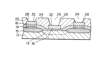
A cross-sectional view of part of a integrated
circuit structure 10 at successive steps during a method of
tapering sidewalls of via holes according to an embodiment
of the present invention is shown in Figure 1. The
structure 10 comprises a substrate in the form of part of a
semiconductor wafer 12, having elements 13, 14 and 15 of
CMOS device structures defined thereon, an overlying
insulating dielectric layer of borophosphosilicate glass
(BPSG) 20, and a first conductive metal layer, comprising
portions 16 and 18 forming interconnects which are
vertically spaced apart because the underlying topography
is non-planar. The portions 16 and 18 of interconnect are
separated by a further layer of insulating dielectric 22,
e.g. a layer of silicon dioxide. Vias holes 24 and 26 of
different depths, having steep sidewalls 28 are defined
through the insulating layer of silicon dioxide 22 and
expose portions of the metal layer at the bottom of each
via hole.
The steep-sided via holes 24 and 26 are provided by
a known conventional method, for example, a step of
selectively masking the insulating layer 22 by coating with
CA 02064922 1998-03-12
photoresist, patterning the photoresist to leave exposed
regions of the insulating layer, and anisotropically
etching exposed regions to define via holes with steep
sidewalls 28. Where the insulating layer 22 is silicon
dioxide a suitable known anisotropic etch is provided by
reactive ion etching using an etch gas mixture of CHF3/O2 in
a commercially available reactive ion etch (RIE) reactor.
The underlying metal interconnect layers 16 and 18 serve as
an etch stop at the bottom of the via holes. Thus, where
exposed regions define circular areas, anisotropic etching
provides a round via hole having a uniform lateral critical
~;m~n~ion, i.e. diameter, and a sidewall of cylindrical
form. Thus, after removing the photoresist, the substrate
is provided with a plurality of steep-sided via holes of
different depths through the insulating layer 22 having a
predetermined uniform bottom diameter cd which is defined
lithographically (i.e. in the step of patterning the
photoresist).
After cleaning the sidewalls with an organic
photoresist stripper, the steep-sided via holes of
different depth are tapered using the following steps. A
thin film of a predetermined thickness of ~120nm to ~150nm
of a protective layer 30, preferably the same material as
the insulating layer 22, i.e. silicon dioxide, is deposited
overall. The protective layer 30 of silicon dioxide is
deposited by a conventional method of chemical vapour
deposition, CVD, to form a thin protective layer of
substantially uniform thickness extending all over the
surface of the dielectric layer 22, on the sidewalls 28 and
on the bottom 32 of the via holes 24 and 26 over the
conductive layer. For example, a process using chemical
reaction between tetraethoxysilane (TEOS) and ~2 in a
commercially available reactor, an Applied Materials CVD
5000 System, was found to give uniform coverage under the
following process conditions: pressure 9 Torr, power 420
Watts, temperature 390 C, gap between electrodes 185 mil,
TEOS flow rate 500sccm, ~2 flow rate 400sccm. The
CA 02064922 1998-03-12
11
deposition time for a 150nm layer of protective oxide was
12 seconds.
The resulting structure is then sputter etched to
remove the layer 30 of ~150nm SiO2 from the via holes 24 and
26, using an argon ion etch. The argon sputter etch
results in removal of the protective layer of SiO2 from the
surface of the insulating layer 22 and from the sidewalls
28 and the bottom 32 of the via hole, while simultaneously
material is also sputtered from the upper peripheral edge
o 36 of the surface 34 of the insulating layer 22 around each
via hole and from the sidewalls 28 of the via holes,
thereby tapering the sidewalls as shown in Figure lc. The
argon sputter etch is carried out in suitable commercially
available sputter etch apparatus. As an example, using the
etch chamber of the Applied Materials CVD 5000 System, a
suitable argon ion etch process was operated at a pressure
of 27 mTorr, an argon gas flow rate of 50sccm, RF power of
450 Watt, and magnetic field of 80 Gauss, to remove 140nm
of a protective layer of silicon dioxide in 200 seconds.
The thickness of the protective layer 30 is an
order of magnitude thinner than the thickness of the
insulating layer, which may be -1-2~m thick. The
protective layer 30 functions as sputter etch stop to
protect the metal in the bottom of the via hole from
sputter damage, and thus to prevent removal of or damage to
the metal in the bottom of the via hole during sputter
etching and tapering of the sidewalls. The etch rate of a
sputter etch is dependent on the angle of incidence of
etchant ions on the surface to be etched. Thus, the
angular dependence of the etch rate of the sputter etching
process provides that the peripheral edge 36 of the
sidewalls 28 of the insulating layer are etched back a
faster rate in an angular direction, so as to taper the
sidewalls, the peripheral edge of the via hole being etched
back in a horizontal direction as viewed in Figure lc,
while the protective layer within the via hole is etched in
relatively slowly in a vertical direction to expose the
CA 02064922 1998-03-12
underlying conductive layer 16 or 18 at the bottom of the
via hole, the protective layer also being removed from the
upper surface 34 of the insulating layer around the via
hole. Thus by suitable selection of the predetermined
thickness of the protective layer, while the protective
layer is sputter etched from the conductive layer, the
peripheral edges 36 and the sidewalls 28 of the via holes
are etched relatively rapidly in an angular direction to
form a desired smoothly tapered sidewall.
o The protective layer functions as an etch stop for
the conductive layer, and is sacrificial, being removed
during the sputter etching step, but protecting the
conductive layer from sputtering damage. However, after
sputtering, some sputtered material may be left in the via
hole. Part of the protective layer may not be completely
removed and a very thin film of the protective layer may
remain in the via hole.
Where electrical contacts are to be formed within
a via hole defined in silicon dioxide, sputtered debris
from sidewalls of the via hole or a residual part of the
protective layer may interfere with formation of a reliable
electrical contact within the bottom of the via hole.
Thus, any sputtered material remaining in the via hole is
cleaned by a short reactive ion etch to expose a clean
conductive layer within the via hole e.g. by exposure to a
plasma generated from a fluorine containing gas. Any
r~m~'n;ng part of the protective layer is removed during
ion etching. The fluorine containing gas may be selected
from CF4, CHF3, C2F6 or SF6. For example, using the Applied
Materials CVD 500 system, ion etching for 36 seconds using
a CF4 gas mixture with typical operating conditions of
pressure 200 mTorr, power 600 Watt, CF4 flow rate 120sccm,
was found to remove sputtered material (debris) from the
bottom of the via hole.
In application of the method according to the
embodiment for sidewall tapering, deep and shallow via
holes may be uniformly tapered simultaneously, after
'~ '
CA 02064922 1998-03-12
deposition of a thin protective layer of oxide, by a
sputter etch step, followed by a brief clean up by reactive
ion etching. No heat treatment or multiple masking
processes are required. Conveniently, deposition of the
protective layer, argon sputter etching, and the RIE clean-
up step are performed in a single pass through the multi-
chamber Applied Materials CVD 5000 System. Alternatively
these process steps may be performed in separate passes
through other appropriate single chamber CVD and etch
o systems.
Although sputtering is well known to provide an
angularly dependent etch rate, where a controlled amount of
etching in a particular direction can be obtained, sputter
etching processes are usually considered too aggressive and
damaging for defining features of small ~impn~ions such as
sub-micron via holes. Generally, a sputter etch would tend
to damage an unprotected conductive layer within the via
hole, and damage other exposed and unprotected substrate
materials, and leave sputtered debris from these materials
in the via hole. However, in the method of the e-m-bodiment~
the damaging effects of sputter etching are circumvented by
deposition of a thin protective oxide layer of a
predetermined thickness before sputter etching. It was
found to be advantageous in obtaining a via hole having a
smoothly tapered sidewall, to clean the steep sidewall
prior to deposition of the protective layer. This was
accomplished with a wet cleaning step, for example, using
an organic photoresist stripper, to remove any traces of
photoresist remaining on the steep sidewalls, before
depositing the protective layer. To provide a clean
conductive surface for formation of contacts within a via
hole, sputter etching is advantageously applied in
combination with a subsequent reactive ion etch or other
cleaning step, to remove any sputtered debris from the via
hole and expose the conductive surface within the via hole.
Thus the method according to the e-mbodiment provides a
controllable process which is applicable to defining
CA 02064922 1998-03-12
14
smoothly tapered sidewalls for via holes of large depth
differential.
It will ~e clear that above-mentioned process
conditions are given by way of example. The method of the
invention may be applied to tapering sidewalls of steep-
sided via holes provided in insulating layers formed by
other known processes. Furthermore, the operating
conditions for the deposition of the protective layer,
argon sputter etch and reactive ion etch may be varied
o within conventional known ranges, dependent on equipment,
to adapt the method of the invention to the particular
materials used for the insulating layer and the protective
layer, while remaining within the scope of the invention.
The resulting tapered via holes may be filled with
a conductive material, for example, an aluminium alloy,
deposited by a conventional known method to form a
conductive interconnect structure. A fully planarized
topography may be achieved with multi-level metal
interconnect structures as illustrated in Figure 2 and 3.
Figure 2 shows the same parts of an integrated circuit
structure as in Figure 1, at a later stage of processing,
after formation of a conductive interconnect structure 40
and deposition of an overlying passivation layer 42. The
interconnect 40 is in the form of metal lines formed by
sputter deposition of aluminium alloy to fill the via
holes. The resulting second level metal lines 40 extend
into the via holes 24 and 26 and provide electrically
conductive contacts at interfaces 44 with portions 16 and
18 of the underlying first metal layer.
Figure 3 includes others parts of the integrated
circuit of Figures 1 and 2, after a further stage of
processing, including another third level of interconnect
50. The interconnect 50 comprises a third level of metal
(ie. aluminium alloy) extending into tapered via holes 52
through dielectric layer 42. The tapered via holes 52 are
formed in the same way as tapered via holes 24 and 26 by
the method according to the embodiment. Thus the third
'' ~
-
CA 02064922 1998-03-12
_ 15
layer metal 50 forms electrically conductive contacts at
interfaces 54 with underlying second level metal layer 40,
and a fully planarized topography is achieved.
The smoothly tapered sidewalls providing for
excellent step coverage in both the shallow and deep via
holes. The lateral critical ~;mensions~ i.e. diameters of
both the deep and shallow holes are almost identical, the
m;n;mllm diameter of each of the shallow and deep via holes
being respectively the same, and sidewalls of the deep and
o shallow via holes being continuously, smoothly tapered.
The cross-sectional profiles of deep and shallow via holes
differ only in depth and the slope of the taper of the
sidewalls.
The method of the present invention and the
resulting tapered via hole structure is particularly
applicable for sidewall tapering of via holes for
multilevel metal interconnect structures for integrated
circuits because via holes of a wide depth differential,
extending through different thicknesses of an insulating
layer, are simultaneously and evenly tapered to provide
e~uivalent cd (diameter) at the bottom of both deep and
shallow via holes. Design rules for m; nlmllm line width at
each level of metal are thus simplified. Sidewall tapering
of very deep via holes to the bottom of the via holes may
be achieved. In particular, the method is found to provide
superior step coverage for via holes having a depth
differential of ~0.5~m, and provides substantially uniform
cds, without significant blooming of shallow via holes.
.~ ,
, ,