Note : Les descriptions sont présentées dans la langue officielle dans laquelle elles ont été soumises.
CA 0206~894 1997-0~-28
2065894
DATA TRANSFER SYSTEM
FIELD OF THE INVENTION
This invention relates to a data transfer
system, and more particularly to, a data transfer
system using an auto-increment-pointer.
BACKGROUND OF THE INVENTION
A conventional data transfer system, using an
auto-increment-pointer, includes a plurality of
central processors, an I/O panel having a buffer, an
internal pointer and an external pointer, and a system
bus connecting between the central processors and the
I/O panel. The buffer includes a predetermined
number of buffer areas accessed by the central
processors and the I/O panel. The external pointer
stores an initial address for access to the buffer
areas by the central processors and the internal
pointer stores an initial address for access to the
buffer areas only by the I/O panel. The priority is
decided among the central processors by a bus
arbitration circuit.
In the conventional data transfer system,
when the external pointer is read by one of the
central processors which is selected by the bus
arbitration circuit, an address data stored in the
!j
CA 0206~894 1997-0~-28
2 206~89~
external pointer is supplied to the central processor.
Then, a predetermined data block is transferred from
the central processor to the buffer area in write
mode designated the address data of the external
pointer. At this time, in the external pointer, an
address value "l" is automatically added to the
precedent address data, and the added address is
stored in the external pointer as a subsequent
address. In the same manner, read mode is carried out
between the central processors and the I/O panel.
On the other hand, when the internal pointer
is accessed by the I/O panel, a predetermined data
block is transferred from the buffer, for instance,
to a periphery circuit in accordance with an address
data stored in the internal pointer.
According to the conventional data transfer
system, however, there are disadvantages in that when
a transferred data block has a length longer than
that of the buffer areas, the data block has to be
divided so that the divided data is shorter than the
length of the buffer areas, because the length of the
buffer areas is fixed to be a predetermined length.
As a result, a transfer speed is low. On the other
hand, if a length of a transferred data block is
shorter than that of the buffer area, a portion of
the area is useless in the buffer.
CA 0206~894 1997-0~-28
3 2065894
SUMMARY OF THE INVENTION
Accordlngly, lt ls an ob~ect of the lnventlon to
provlde a data transfer system whlch operates with high speed.
It ls another ob~ect of the lnventlon to provlde a
data transfer system ln whlch a buffer can be used
efflclently.
It ls a further ob~ect of the invention to provlde a
data transfer system ln which a data block stored in the
buffer can be read from lts initial point at any time.
According to the invention, there ls provided a data
transfer system, comprlslng: a plurallty of processors each
havlng predetermlned data blocks to be transferred; a buffer
havlng a predetermined number of buffer areas for storlng data
transferred from sald plurallty of processors; an external
pointer storing an address designatlng a position of one of
said buffer areas ln sald buffer, a system bus connectlng sald
plurallty of processors to sald buffer; means for provldlng
arbltratlon of sald system bus to allow only one of said
plurallty of processors to access said buffer; means for
retrlevlng the address stored ln the external polnter;
means for lncludlng a plurallty of blts corresponding to a
size of data to be transferred from said one of sald plurallty
of processors wlth the address stored ln the external pointer;
means for renewing the address stored ln the external pointer
and read therefrom in accordance with the plurallty of blts
lndicatlve of the slze of data and the address read therefrom;
and means for provlding a data storing area of a predetermined
71885-26
CA 0206~894 1997-0~-28
20658q4
3a
length in sald buffer in accordance wlth the slze of data;
whereln when any of sald plurallty of processors accesses the
external polnter to wrlte data to sald buffer, the address
stored ln the external polnter ls read out and lncremented by
a dlgltal value correspondlng to the plurallty of blts which
are lncluded wlth the address by the renewlng means.
In accordance wlth the present inventlon, there ls
provided a data transfer system, comprislng: a plurallty of
central processors each controlllng a transfer of a data
block; a buffer memory for storlng data blocks transferred
through a system bus from sald plurallty of central
processors; a bus arbltratlon clrcult for arbltratlng a use of
sald system bus by one of sald plurallty of central
processors; and a polnter for storlng a buffer-address
deslgnatlng an lnltlal address of sald buffer memory in sald
transfer of said data block; wherein said one of said
plurality of central processors accesses said pointer to read
said buffer-address by using an address signal includlng a
pointer-address for designating said pointer and an increment
data proportlonal to a block length of sald data block; sald
pointer adds sald buffer-address stored thereln and said
increment data to generate a renewing buffer-address, and
stores sald renewlng buffer-address in place of said buffer-
address read by said one of said plurality of central
processors; and said one of said plurality of central
processors transfers said data block to said buffer memory by
using said buffer-address read from said pointer.
71885-26
CA 0206~894 1997-0~-28
206589~
3b
In accordance with the present lnventlon, there ls
further provlded a method for transferrlng data from one of a
plurallty of processors to a buffer, sald buffer lncludlng a
plurallty of buffer areas and an external polnter that ls used
to point to one of said plurality of buffer areas, comprising
the steps of: a) determining a block length of a block of data
to be transferred to said buffer from said one of sald
plurallty of processors; b) supplylng a predetermlned signal
from sald one of sald plurality of processors to the external
pointer in preparation for transfer of said block of data to
said buffer; c) supplying an address stored ln the external
polnter to said one of said plurality of processors in
response to said predetermined signal, said address indicative
of one of said buffer areas ln whlch said block of data is to
be stored within said buffer; d) detecting, by said one of
said plurality of processors, a size of said block of data to
be transferred to said buffer; e) calculating an auto-
lncrement value ln accordance wlth the slze of sald block of
data to be transferred to sald buffer, whereln a new address
to be supplled to the external polnter is generated as a
result thereof; f) wrltlng the block of data to sald buffer at
the address stored ln the external polnter; and g) renewing
the external pointer with the new address for a next data
transfer to said buffer by any of said plurallty of
processors.
BRIEF DESCRIPTION OF THE ~RAWINGS
71885-26
CA 0206~894 1997-0~-28
20~894
The invention will be explained in more
detail in conjunction with appended drawings;
wherein:
Fig. 1 is a block diagram showing a data
transfer system of a preferred embodiment according to
the invention;
Fig. 2 is a format of a data transferred from
a central processor to an I/O panel in the preferred
embodiment;
Fig. 3 is a format of a data block
transferred from a central processor to a buffer in
the preferred embodiment;
Fig. 4 is an explanatory view showing
operation Or the I/O panel (an external pointer) of
the preferred embodiment;
Fig. 5 is a memory map of a two-port RAM used
in the preferred embodiment;
Fig. 6 is a block diagram showing an external
pointer used in the preferred embodiment;
Figs. 7 and 8 are flow charts showing
operation of the preferred embodiment; and
Fig. 9 is a format of a data stored in the
buffer.
DESCRIPTION OF THE PREFERRED EMBODIMENTS
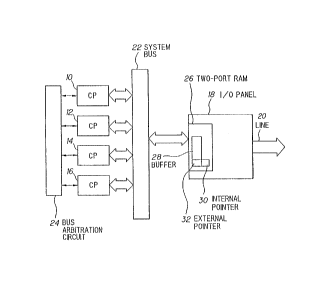
Fig. 1 shows a data transfer system of a
preferred embodiment according to the invention. The
.,
CA 0206~894 1997-10-28
data transfer system includes four central processors 10, 12,
14 and 16, an I/O panel 18 connected to a line 20, a system
bus 22 connecting between each of the central processors 10,
12, 14 and 16 and the I/O panel 18, and a bus arbitration
circuit 24 connected to the central processors 10, 12, 14 and
16, respectively.
The bus arbitration circuit 24 controls the central
processors 10, 12, 14 and 16 to access to the I/O panel 26
without a confliction among them. The I/O panel 18 includes
a two-p~rt RAM 26 having a buffer 28, and internal and
external pointers 30 and 32 storing address data PTRi and PTRe
for access to the buffer 28 by the central processors 10, 12,
14 and 16 and the I/O panel 18, respectively. Each of the
central processors 10, 12, 14 and 16 supplies an increment
data "Lb" corresponding to a length of a transferred data
block to the external pointer 32 in addition to the address
data PTRe, so that a data 100 is obtained as shown in Fig. 2.
At the same time, each of the central processors 10, 12, 14
and 16 transfers a data block including a buffer busy fla~
"B", a header "HEADER" and a length data "Li" of the trans-
ferring data block to the buffer 28 as shown in Fig. 3. The
header "HEADER" is determined to be a different value relative
to the other data blocks to avoid a confusion among them.
The address data PTRe is renewed in the addition of the
increment data "Lb" thereto as shown in Fig. 4.
Fig. 5 shows a memory map of the two-port RAM 26
having two aspects for the I/O panel 18 and for the system
71885-26
CA 0206~894 1997-10-28
bus 22. That is, for the I/O panel 18, the two-port RAM 26
has addresses $0000 to $7FFF to be composed of a RAM area
having addresses $8000 to $FFFF. On the other hand, for the
system bus 22, the two-port RAM 26 is composed of a buffer
area 28E, an external pointer area 32E and an internal pointer
area 30E corresponding to the buffer 28, the external pointer
32 and the internal pointer 30, respectively, as shown in
Fig. 1.
The buffer area 28E is accessed in read and write
modes by the central processors 10, 12, 14 and 16. The
external pointer area 32E stores an address data for access
to the buffer area 28E, and is accessed in read and write modes
by the central processors 10, 12, 14 and 16. When the
presently stored address is read by the central processor 10,
12, 14 or 16, the address data is renewed automatically in
accordance with the increment data "Lb" for the subsequent
access to the buffer area 28E. The internal pointer area 30E
can not be accessed by the central processors 10, 12, 14 and
16, while it is accessed only by the I/O panel 18.
Fig. 6 shows the external pointer 32 including a
timing controller 40 supplying timing signals RWS, RDGATE,
LATCH, INGATE and WSEL, a decoder 42 for decoding an address
signal, a gate 44 for controlling the transfer of data, a
RAM 46 for storing a predetermined data, a latch circuit 48
connected between the gate 44 and the RAM 46 for latching a
signal read from the RAM 46, an adder 50 for adding the read
71885-26
CA 0206~894 1997-10-28
address data A and an increment data B, a selector 52 for
selecting an input signal between X and Y to write an output
signal Q to the RAM 46, and an address controller 54 for
masking the increment data "Lb" of the data 100.
The I/O panel 18 including the external pointer 32
operates in first and second modes. The first mode is carried
out as an ordinary operation, when an address signal is
decoded in the decoder 42 for access to addresses other than
an address assigned to the external pointer 32, and the second
mode is carried out as a specified operation to embody the
invention, when an address signal is decoded therein for
access to the address signal assigned to the external pointer
32.
(a) FIRST MODE
In writing mode, the gate 44 is closed and the
input Y of the selector 52 is opened, so that a predetermined
data is supplied to the RAM 46 through the selector 52. In
reading mode, a data stored in the RAM 46 is supplied to the
system bus 22 through the latch circuit 48 and the gate 44.
(b) SECOND MODE
Here, it is assumed that the central processor 10
is selected to access to the exterior pointer 32 by the bus
arbitration circuit 24. An address signal designating the
RAM 46 assigned to the external pointer 32 is supplied to an
address bus to be connected to the decoder 42. An AINC (auto-
increment) signal is generated in the decoder 42 to be
71885-26
CA 0206~894 1997-10-28
supplied to the controller 40 by decoding the address signal
excluding lower eight bits assigned to an auto-increment data,
so that the gate 44 and the latch circuit 48 become opened.
Thus, an address data stored in the RAM 46 is supplied to the
central processor 10 through the latch circuit 48 and the
gate 44. The increment data "Lb" is supplied to the address
bus together with the read address signal. At the same time,
the read address data is latched at the latch circuit 48 to
be supplied to the input A of the adder 50, so that the
address data is added with the increment data "Lb" supplied
from the address bus to the input B of the adder 50. The
added data is supplied through the selector 52 to the RAM 46,
so that the added data is stored therein as a renewal address
data. Finally, a signal DTACK indicating a finish of the
access is supplied from the controller 40 to the central
processor 10. The central processor 10 transfers the data
to be written to the buffer 28 by accessing to the address
supplied from the external pointer 32.
Next, this described operation will be again
explained in conjunction with Figs. 7 to 9.
In Fig. 7, it is also supposed that the central
processor 10 is selected by the bus arbitration circuit 24.
When the selected signal is supplied from the bus arbitration
circuit 24 to the central processor 10, the central processor
10 supplies a predetermined signal to the external pointer 32.
In response to the signal supplied from the central processor
71885-26
CA 0206~894 1997-10-28
10, an address data PTRe stored in the external pointer 32
is supplied to the central processor 10. At the same time,
the central processor 10 detects a block length "Li" cf a
transferred data block (S31), and an auto-increment data
"Lb" is calculated in accordance with the block length "Li"
(S32) to produce an address signal 100 including the increment
data "Lb" as shown in Fig. 2. For example, if it is supposed
that the minimum storing bit length of the external pointer
32 is sixty-four bits, the block length "Li" is divided by
sixty-four. Then, an integer value of the divisional
calculation result is added to the value "1" to provide the
increment data.
Next, the renewal data 100 is supplied from the
central processor 10 to the external pointer 32 through the
system bus 22 (S33). The increment data "Lb" is added to
the read and latched address data, so that a subsequent
address data representing an initial address of a subsequent
data transferred from another processor is stored therein
instead of the precedent address data.
After that, an initial address of the data block is
determined in accordance with the data of the external
pointer 32 (S34), so that the data block is transferred from
the central processor to the buffer 28 (S35). When the data
transfer is finished, the buffer busy flag "B" becomes "1"
(S36).
71885-26
CA 0206~894 1997-10-28
Fig. 8 shows a flow chart of the preferxed embodi-
ment in a case that a predetermined data stored in the buffer
28 is supplied to the line 20 by using the internal pointer
30. When an initial address of a transferred data block is
designated in accordance with an address data PTRi stored in
the internal pointer 30 (S41), a header "HEADER" is judged to
be set or not at a position having a predetermined relation
to the detected initial address (S42). When the header
"HEADER" is detected as shown in Fig. 9 at "a" and "b", the
buffer busy flag "B" is judged to be set to be "1" or not
(S43). When the buffer busy flag "B" is set to be "1", the
data block is read from the initial address and is transferred
to the line 20 (S44). If the buffer busy flag "B" is not set
to be
71885-26
2 ~ 4
"1", the data block is not read until the busy flag
becomes "1". When the transfer is rinished~ the
buffer bllsy flag ~n~ Is reset to be "O" (S45), the
precedent address data PTRi of the internal poInter
30 is renewed in accordance with the block length
"Li", and baclc to the step $41.
If the address data PTRi stored in the
internal pointer 30 designates a midpoint of the data
block, at which a header "IIEADER" is not detected as
shown in Fig. 9 at "c", a header "IIEADER" is searched
in the buffcr 28 (S~7~, the wrong address data is
amended in accordance with a position of the searched
header "IIEADER" (S48), and back to the step S41.
As described above, according to the
preferred embodiment, the address data PTRe of the
external pointer 32 is renewed in accordance with a
length of a transferring data block, so that the data
block can be transferred at one time. TherePore,
operating speed o~ the system becomes high. Further,
there is decreased useless area in each of the buffer
areas, so that the blIffer 28 can be used ef~iciently.
In additioni the transferring data block
includes a header "IIEADE~", so that a data block
stored in the buffer can be read from its initial
25 , point at any time.
Although the invention has been descrihed
with respect to speci~ic embodiment ~or complete and
li
. . ~
12
2~3~9~
clear disclosure, the appended claims are not to be
thus limited but are to be construed as embodying all
modification and alternative constructions that may
occur to one skilled in the art which fairly fnll
withill the basi¢ teaohillg llcreill set fortll.
.
,~ .
~ 20
'
~!
' ' ' - ' ' ' ~
:. : '
:, :