Note : Les descriptions sont présentées dans la langue officielle dans laquelle elles ont été soumises.
BC9-91-0~7 1 2 0 6 6 00
PERSON~L ~Ul~ MEMORY W~ITE CONTROL
Technical Field
This invention relates to personal computers, and more
partlcularly to a personal computer USill~ a small computer
systems interface (SCSI) controller coupled directly to the
local processor bus for controlling data transfer with
storage memory devices such as fixed or removable media
electromagnetic storage devices.
Background of the Invention
Personal computer systems in general and IBM~ personal
computers in particular have attained widespread use for
providing computer power to many segments of today's modern
society. Personal computer systems can usually be defined
as a desk top, floor standing, or portable microcomputer
that consists of a system unit having a single system
processor and associated volatile and non-volatile memory, a
display monitor, a keyboard, one or more diskette drives, a
fixed disk storage, and an optional printer. One of the
distinguishing characteristics of these systems is the use
of a motherboard or system planar to electrically connect
these components to~ether. These systems are designed
primarily to give independent computing power to a single
us0r and are inexpensively priced for purchase by
individuals or small businesses. Examples of such personal
computer systems are the IBM PERSONAL COMPUTER AT~ and IBM
PERSONAL SYSTEM/2~ Models 25, 30, L40SX, 50, 55, 65, 70, 80,
90 and 95.
~ .
These systems can be classified into two general families.
The first family, usually referred to as Family I Models,
use a bus architecture exemplified by the IBM PERSONAL
COMPUTER AT and other i'IBM compatible" machines. The second
family, referred to as Family II Models, use the IBM MICRO
CHANNEL~ bus architecture exemplified by IBM's PERSONAL
SYSTEM/2 Models 50 through 95. The Family I models
typically have used the popular INTEL~ 8088 or 8086
microprocessor as the system processor. These processors
206~
sC9-91-047 2
have the ability to address one megabyte of memory. The
Family II models -typically use the high speed INTEL 80286,
80386, and 80486 microprocessors which can operate in a real
mode to emulate the slower speed INTEL 8086 microprocessor
or a protected mode which e~tends the addressing range from
1 megabyte to ~ Gigabytes for some models. In essencel the
real mode feature of the 802861 80386, and 80486 processors
provide harclware compatibility with software written for the
8086 and 8088 microprocessors.
As the development of personal computers has advanced, there
have been proposals for certain standards to be established
among makers and users of such apparatus for the purpose of
enabling greater exchangability of components and the like.
One such st~ndard which have achieved some broad acceptance
is the small computer systems interface (SCSI) standard for
data communication to and from storage memory devices. For
the present purposes, "storage memory devices" is defined
broadly to include all devices capable of storing data in
digital form, with particular emphasis on such devices as
fixed or removable media electromagnetic storage devices
(also known as hard and floppy disk drives),
electro-optical, tape and other storage devices. SCSI
controllers have been known and used prior to this
invention, and will be familiar to the knowledgeable reader.
In prior personal computer systems, SCSI controllers have
typically been arranged as option or accessory devices,
accessed by the system through the accessory or input/output
or I/O bus. In such arrangements, data transfer rates or
operating speeds are relatively lower. As a consequence, the
provision of data hold times for transfer through gate
devices or drivers was relatively easily accomplished. Two
approaches used to assure appropriate data transfer have
been the provision of additional wait cycles or clocked
intervals to the logic involved, so tha-t extra time was
allowed, and reliance on internal gate delays introduced in
part to assure timing.
It is now contemplated to provide a SCSI controller as a
single very large scale integrated (VLSI) device or
BC9-91-047 3
application speci~ic integrated circuit (ASIC) chip, and to
provide for connection of that controller directly with the
local processor bus. The purpose of so providing such a
controller is to achieve enhanced performance in terms of
expedited data transfers. However, the two approaches
identified above either impair or endan~er s~lch performance.
In particular, the introd~lction of additional states and
clock cycle~ into the arrangement is functional while
imposing an unacceptable performance penalty. Where high
performance is sou~ht, reliance on gate delays is
unacceptably risky as such delays are subject to significant
variation from device to device or over time and in varying
operating conditions.
Brief Description of the Invention
With the foregoing in mind, it is an object of this
invention to provide a VLSI or ~SIC SCSI controller coupled
directly to a local processor bus and capable of high
performance in terms of data transfer. In realizing this
object of the present invention, provision is made for
assuring that sufficient time intervals are employed for
data transfer while avoiding excessi.ve delays or risk of
data loss in such transfers.
A further object of this invention is to provide, in a VLSI
SCSI controller, logic internal to the devic~ which assures
that effective and minimal time data transfers occur. In
realizing this object of the present invention, an enchained
pair of a driver and a receiver are used to pass a memory
write signal to data transfer drivers. The appropriate
assurance of data transfer and avoidance of excessive delay
or risk is achieved by the characteristics of the driver and
receiver.
Brief Description of the Drawings
Some of the objects of the invention having been stated,
other objects will appear as the description proceeds, when
taken in connection with the accompanying drawings, in
which:
20~0~1
BC9-91-047 4
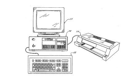
Figure 1 is a perspective view of a personal computer
embodying this invention;
Figure 2 is an exploded perspective view of certain
elements of the personal computer of Figure l including a
chassis, a cover, and a planar board and illustrating
certain relatiorlships among those elements;
Figure 3 :is a schematic view of certain components of
the personal computer o:E Figures 1 and 2; and
Figure ~ is a schematic view of certain components
included in the SCSI controller of the personal computer of
Figures 1 through 3.
Detailed Description of Invention
While the present invention will be described more fully
hereinafter with reference to the accompanying drawings, in
which a preferred embodiment of the present invention is
shown, it is to be understood at the outset of the
description which follows that persons of skill in the
appropriate arts may modify the invention here described
while still achieving the favorable results of this
invention. Accordingly, the description which follows is to
be understood as being a broad, teaching disclosure directed
to persons of skill in the appropriate arts, and not as
limiting upon the present invention.
Referring now more particularly to the accompanying
drawings, a microcomputer embodying the present invention is
there shown and generally indicated at 10 (Figure 1). As
mentioned hereinabove, the computer 10 may have an
associated monitor 11, keyboard l~ and printer or plotter
14. The computer 10 has a cover 15 which cooperates with a
chassis 19 in defining an enclosed, shielded volume for
receiving electrically powered data processing and storage
components for processing and storing digital data, as shown
in Figure 2. At least certain of these components are
mounted on a multilayer planar 20 or motherboard which is
mounted on the chassis 19 and provides a means for
electrically interconnecting the components of the computer
including those identified above and such other
associated elements as floppy disk drives, various forms of
2~60~
BC9-91-047 5
direct access storage devices~ accessory cards or boards,
and the like.
The chassis l9 has a base and a rear panel (Figure 2) and
defines at least one open bay for receiving a data storage
device such as a disk drive for magnetic or optical disks, a
tape backup drive, or the like. In the illustrated form, an
upper bay 22 is adapted to receive peripheral drives of a
first size (such as those known as 3.5 inch drives). A
floppy disk drive, a removable media direct access storage
device capa~le of receiving a diskette inserted thereinto
and using the diskette to receive, store and deliver data as
is generally known, may be provided in the upper bay 22.
Prior to relating the above structure to the present
invention, a summary of the operation in general of the
personal computer system lO may merit review. Referring to
Figure 3, there is shown a block diagram of a personal
computer system illustrating the various components of the
computer system such as the system lO in accordance with the
present invention, including components mounted on the
planar 20 and the connection of the planar to the I/O slots
and other hardware of the personal computer system.
Connected to the planar is the system processor 32. While
any appropriate microprocessor can be used as the CPU 32,
one suitable microprocessor is the 80386 which is sold by
INTEL. The CPU 32 is connected by a high speed CPU local
bus 34 to a bus interface control unit 35, to volatile
random access memor~ (RAM) 36 here shown as Single Inline
Memory Modules (SIMMs) and to BIOS ROM 38 in which is stored
instructions for basic input/output operations to the CPU
32. The BIOS ROM 38 includes the BIOS that is used to
intarface between the I/O devices and the operating system
of the microprocessor 32. Instructions stored in ROM 38 can
be copied into RAM 36 to decrease the execution time of
BIOS.
~1hile the present invention is described hereinafter with
particular reference to the system block diagram of Figure
3, it is to be understood at the outset of the description
which follows that it is contemplated that the apparatus and
BC9-91-047 6 ~ 0~ ~ 0 0 1
methods in accordance with the pres0nt invention may be used
with other hardware confi~urations of the planar board. For
example, the system processor could be an Intel 80286 or
80486 microprocessor.
Returning now to Figure 3, the CPU local bus 34 (comprising
data, address and control components) also provides for the
connection of the microprocessor 32 w:ith a math coprocessor
39 and a Small Computer Systems Interface (SCSI) controller
40. The SCSI controller 40 may, as is known to persons
skilled in the arts of computer design and operation, be
connected or connectable with Read Only Memory (ROM) 41, RAM
42, and suitable external devices of a variety of types as
facilitated by the I/O connection indicated to the right in
the Figure. The SCSI controller 40 functions as a storage
controller in controlling storage memory devices such as
fixed or removable media electromagnetic storage devices
(also known as hard and ~1Oppy disk drives),
electro-optical, tape and other storage devices.
The bus interface controller (BIC) 35 couples the. CPU local
bus 34 with an I/O bus 44. By means of the bus 44, the BIC
35 is coupled with an optional feature bus such as a MICRO
CHANNEL bus having a plurali.ty of I/O slots for receiving
MICRO CHANNEL adapter cards 45 which may be further
connected to an I/O device or memory (not shown). The I/O
bus 44 includes address, data, and control components.
Coupled along the I/O bus 44 are a variety of I/O components
such as a video signal processor 46 which is associated with
video RAM [VRAM) for storing graphic information (indicated
at 48) and for storing image information (indicated at 49~.
Video signals exchanged with the processor 46 may be passed
through a Digital to Analog Converter (DAC) 50 to a monitor
or other display device. Provision is also mada for
connecting the VSP 46 directly with what is here referred to
as a natural image input/output, which may take the form of
a video recorder/player, camera, etc. The I/O bus 44 is
also coupled with a Digital Signal Processor (DSP) 51 which
has associated instruction RAM 52 and data RAM 54 available
to store software instructions for the processing of signals
BC9-91-047 7 20~B~0~
by the DSP 51 and data involved in such processing. The DSP
51 provides for processing of audio inputs and outputs by
the provision of an audio controller 55, and for handling of
other signals by provision of an analog interface controller
56~ Lastly~ the I/O bus 44 is coupled with a input/output
controller 58 with associated ~lectrical Erasable
Programmable Read Only Memory (EEPROM) 59 by which inputs
and outputs are exchanged with conventional peripherals
including floppy disk drives, a printer or plotter 14,
keyboard 12, a mouse or pointing device (not shown), and by
means of a serial port~
Turning now more directly to the characteristics of the
present invention, the SCSI controller 40 has within it
certain circuit elements illustrated in Eigure 4. More
particularly, the controller 40 has control drivers
indicated at 61 interposed between internal volatile memory
or RAM cells provided in the VLSI structure of the device
and the external volatile memory RAM 42 coupled to the
controller 40 for controlling communication of data to the
RAM 42. The storage controller 40 further has an enable
driver 62 and an enable receiver 64 enchained between the
control drivers 61 and a source of signals controlling data
communication. The driver 6~ and receiver 64 are formed as
an output/input cell of the VLSI and replace, functional,
what might otherwise have been an output cell connected with
an output pin of the package for the VLSI and thereby with
the external RAM 42. The enchained driver 62 and receiver
64 are connected for issuing a write signal to the external
RAM 42 prior to enablement of data communication through the
control drivers 61 and for sustaining a control signal
communicated to the control drivers 61 for enabling data
communication until after deactivation of the write signal.
The signal directed to the external RAM issues from a
circuit point between the driver 62 and receiver 64. The
signal directed to the driver 62 and receiver 64 arrives
from within the VLSI structure of the SCSI controller 40,
and is passed from the receiver 64 to the enable port of the
drivers 61 which are interposed between the source of data
to be transferred from the controller 40 to the associated
external RAM 42. The drivers 61 receive data from within
20~60~
BC9-91-047 8
the VLSI structure of the SCSI controller 40 and pass that
data onward (under control as here described) to the
external RAM 42.
By the structure descrlbed above and the cooperation
contemplated, the .tnternal logic of the SCSI controller 40
has knowledge of when the external pin on the device has
reached an inactive state and it is safe to degate the write
data passing through the drivers 61. The drivers 61 (which
gate write data to the RAM ~2) are not enabled until the
write pulse has become active at the RAM, and are not
degated until the write pulse has become inactive at the
RAM. The RAM requires a minimum of a certain number of
nanoseconds of data hold time at the drivers 61. The
present circuit guarantees this minimum, with a guard band
of the delay time in the receiver and the degate time in the
drivers.
Stated differently, the enchained driver and receiver are
connected for delaying the enablement of data communication
through the control drivers after issuance of a write signal
to the external volatile memory by an interval determined by
the delay imposed by the enable receiver and for sustaining
the enablement of data communication through the control
drivers for an interval determined by ihe degate delay
imposed by the control drivers.
The circuit of the present invention has another advantage,
important in some packaging. That is that it saves pins as
compared ~ith any alternative circuit which would use
"output enable" signals exchanged with the RAM.
In the drawings and specifications there has been set forth
a preferred embodiment of the invention and, although
specific terms are used, the description thus given uses
terminology in a generic and descriptive sense only and not
for purposes o~ limitation.