Note : Les descriptions sont présentées dans la langue officielle dans laquelle elles ont été soumises.
DMR082691 PATENT
014OM Dkt. No. 9lA262
_
ZQ~ 7
ELECTRON BEAM GUN
FOR USE IN AN ELECTRON BEAM EVAPORATION SOURCE
BACKGROUND OF THE INVENTION
The present invention relates to an electron beam gun for
an electron beam evaporation source of the type used in
depositing a thin film of evaporated material onto a
substrate. More particularly, the present invention relates to
such an electron beam gun in which a beam former used in
generating a ribbon-like electron beam to melt and evaporate
the material is formed in two sections that are separately
connected to a split cathode block to prevent thermal
deformation of the beam former. The prevention of thermal
deformation of the beam former increases the service life the
electron beam gun.
In the prior art, electron beam evaporation sources employ
an electron beam gun located beneath a crucible containing a
material to be evaporated. The evaporated material is
subsequently deposited onto a substrate held above the
evaporation source. In such evaporation sources, the electron
beam gun emits a ribbon-like beam that is magnetically
deflected through an arc of 270 and into the crucible to melt
and evaporate the material.
The electron beam gun employs a filament connected to a
split cathode block having two sides. An anode having a top
T
DMR082691 PATENT
014OM Dkt. No. 9lA262
_ - 2 - 2~`57
section of 'U' shaped cross-section passes over the filament
and terminates in a front edge spaced from and located in front
of the filament . The beam former is located between the anode
and the filament and is configured so that the filament is
shielded from the anode. When an electrical current is applied
to the filament through the cathode block, the filament emits
electrons which because of the shielding of the beam former are
constrained to pass beneath the beam former and toward the
front edge of the anode in a ribbon-like electron beam. By the
time the electrons reach the anode a sufficient kinetic energy
has been imparted to the electrons to cause the electrons to
miss the anode and thereby to be emitted from the electron beam
gun. The ribbon-like beam emitted by the electron beam gun is
deflected by magnetic pole pieces of the evaporation source
into the crucible.
The beam former, which has essentially the same shape of
the anode, is connected to one of the sides of the cathode
bloc~ and insulated from the other of the sides of the cathode
block by an insulator. The cathode block acts as a heat sink
to the beam former, but since the beam former is only connected
to one side of the cathode block, a thermal gradient is
produced across the beam former. The resultant unequal heat
distribution within the beam former causes the beam former to
warp and move. Such warpage and movement can cause the beam
former to rise above the lower front edge of the anode and thus
cause electrons to directly arc into ~he anode, destroying the
anode. In addition, the warpage and movement of the beam
former can deform the beam. Such deformation can change the
impact area, and thus, produce a non-uniform evaporation of the
material to be evaporated.
As will be discussed, the present invention provides an
improved electron beam gun in which the beam former and its
attachment to the cathode block are designed to prevent the
production of thermal gradient across the beam former to in
DMR082691 PATENT
0140M Dkt. No. 91A262
.
_ 3 _ 2a7~4~7
turn prevent warpage and movement of the beam former.
~UMMARY OF THE INVENTION
The present invention provides an electron beam gun for use
in an electron beam evaporation source. The electron beam gun
includes a split cathode block having two electrically
conductive sides. A filament is con~ected to the two sides of
the cathode block so that an electric current applied to the
two sides of the cathode block causes the filament to emit
electrons. An anode is provided to accelerate the electrons.
The anode has an outer top section of 'U' shaped cross-section
passing over the filament and terminating in a front edge
located in front of the filament. A beam former is located
between the anode and the filament and is configured so that
the filament is shielded from the anode and the electrons are
constrained to pass beneath the beam former and toward the
anode in a ribbon-like electron beam. The beam former is
fabricated in two sections with a vertical gap between the
sections. The two sections are separately connected to the two
sides of the cathode block such that the two sections of the
beam former are in good thermal contact with the two sides of
the cathode block and the two sides of the cathode block act as
a heat sink for the two sections of beam former. As a result,
a non-uniform thermal gradient is not produced within the beam
former which can cause warpage and movement of the beam
former. The gap is sized such that the electrons emitted from
the filament cannot pass through the gap directly to the anode.
BRIEF DESCRIPTION OF THE DRAWINGS
While the specification concludes with claims distinctly
pointing out the subject matter that Applicants regard as their
invention, it is believed the invention will be better
DMR082691 PATENT
0140M Docket No. 91A262
~ 4 2~ )4.S~
understood from the following description taken in conjunction
with the accompanying drawings, in which:
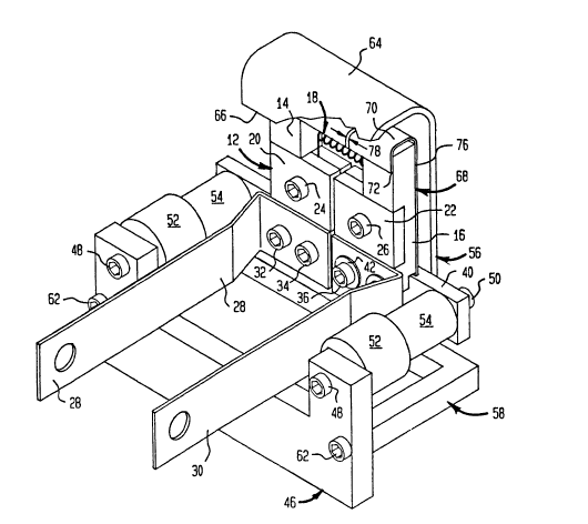
FIG. 1 is a perspective view of an electron beam gun in
accordance with the present invention with portions of an anode
thereof broken away to illustrate a beam former used in forming
an electron beam;
FIG. 2 is a a front view of FIG. l;
FIG. 3 is a sectional view of FIG. 2 taken along line 3-3
of FIG. 2; and
Fig. 4 is a rear view of FIG. 1 with portions of the anode
broken away.
DETAILED DESCRIPTION OF THE DRAWINGS
With reference to the figures, an electron beam gun 10 in
accordance with the present invention is illustrated. Electron
beam gun 10 is a modified electron beam gun known to those
skilled in the art and widely used in 270 electron beam
evaporation sources.
Electron beam gun 10 is provided with a cathode block 12
having two conductive sides 14 and 16 spaced slightly apart
from one another. A filament 18 is connected to sides 14 and
16 of filament block 12 by two filament clamps 20 and 22,
affixed to the two sides 14 and 16 of cathode block 12 by
screws 24 and 26. Two filament bus bars 28 and 30 are in turn
connected to sides 14 and 16 of filament block 12 to apply an
electric current across sides 14 and 16 of cathode block 12,
and thus, filament 18. The electric current causes filament 18
to emit electrons.
Filament bus bars 28 and 30 are in turn connected by screws
32, 34, 36 and 38 to mounting bar 40. Cathode block 12 is
insulated from mounting bar 40 by provision of 2 sets of
insulative washer pairs 42 and 44, through which screws 36 and
DMR082691 PATENT
0140M Dkt. No. ~lA262
20 ~45
-- 5 --
38 e~tend. As may be appreciated, one of the filament blocks
must be insulated from mounting bar 40 to prevent sides 14 and
16 of cath~de hloc~ ~2 from being shunted. Mounting bar 40 is
in turn connected at its enas to a support bar 46 by screws 48
and 50 which pass t~rough insulator pairs 52 and S4. Insulator
54 slides into shield 52 in a manner well known in the art.
An anode 56 is provided to accelerate electrons emitted by
filament 18. Anode 56 is connected at the bottom to anode
mounting bracket 58 by screws 60. Anode mounting bracket 58,
at its ends, is in turn attached to support bar 46 by screws
62. Anode 56 has a top portion 64 of 'U' shaped configuration
which terminates in a front edge 66 located in front of
filament 18.
A beam former 68 is provided. Beam former 68 is configured
to shield filament lB from anode 56. In this regard, beam
former 68 is located between filament 18 and anode 56, and has
essentially the same shape as anode~ 56. That is, it has a top
portion 70 of 'U' shaped configuration terminating in a lower
edge 72 located between lower edge 66 of anode 56 and filament
18.
The shielding provided by beam former 68 causes electrons
emitted by filament 18 to form an electron cloud under top
portion 70 of beam former 68. As a result, a virtual cathode
is formed from which electrons pass beneath lower edge 72 of
beam former 68 in a flat ribbon-like configuration toward lower
edge 66 of anode 56. By the time electrons reach lower edge 66
of anode ~6, a sufficient kinetic energy has been imparted such
that the ribbon-like beam misses anode 56 and is emitted from
electron beam gun 10.
In the prior art, beam former 68 was formed in a single
section and was connected to side 14 of cathode block 12. The
other side of beam former 68 was insulated from side 16 of
DMR082691 PATENT
0140M Dkt. No. qlA262
2~ 57
cathode block 12 to prevent cathode block 12 from being
shunted. The end result of this was that a thermal gradient
was pr~duced within beam former 68 in which beam former 68 was
coolest at it~ attachment to side 14 of cathode block 12, and
hottest at the insulator, insulating beam former 68 from side
16 of cathode block 12.
The thermal gradient wa6 found to cause warpage and
movement of beam former 68. For instance, rotational mo~ement
of beam former 68 caused lower front edge 72 thereof to raise
itself above lower front edge 66 of anode ~6 to in turn cause
electrons emitted from filament 18 to directly arc and strike
anode 56, resulting in its eventual destruction. Other
rotational movements caused deformation of the ribbon-like beam
to produce non-uniform evaporation as electron beam gun aged
over its surface life.
In order to prevent this, in electron beam gun 10, beam
former 68 is formed in two sections 74 and 76 separated by a
~ap 78. Sections 74 and 76 of beam former 68 are separately
connected to sides 14 and 16 of cathode block 12 by screws 80
and 82. Although not illustr~ted, anode 56 is provided with
apertures to accommodate the screw heads of screws 80 and 82.
The spacing of gap 78 is critical. For instance, if gap 78
were too wide, electrons wou~d ~low directly to anode 56. It
has been found by the inventors herein that such gap in an
electron beam gun designed to operate between 4 and 11 KV, at
between a~out 3 and 20 KW, should be between about 0.127 mm.
and a~o~e and leææ than 0.254 mm., with 0.254 mm. being
preferred.
While a preferred embodiment of the invention has been
shown and described in detail, it will be readily understood
and appreciated by those skilled in the art, that numerous
omissions, changes and additions may be made without departing
from the spirit and scope of the in~ention.