Sélection de la langue

Search

Sommaire du brevet 2071697 

Énoncé de désistement de responsabilité concernant l'information provenant de tiers

Une partie des informations de ce site Web a été fournie par des sources externes. Le gouvernement du Canada n'assume aucune responsabilité concernant la précision, l'actualité ou la fiabilité des informations fournies par les sources externes. Les utilisateurs qui désirent employer cette information devraient consulter directement la source des informations. Le contenu fourni par les sources externes n'est pas assujetti aux exigences sur les langues officielles, la protection des renseignements personnels et l'accessibilité.

Disponibilité de l'Abrégé et des Revendications

L'apparition de différences dans le texte et l'image des Revendications et de l'Abrégé dépend du moment auquel le document est publié. Les textes des Revendications et de l'Abrégé sont affichés :

  • lorsque la demande peut être examinée par le public;
  • lorsque le brevet est émis (délivrance).
(12) Brevet: (11) CA 2071697
(54) Titre français: PILE SOLAIRE MINCE
(54) Titre anglais: THIN SOLAR CELL
Statut: Périmé
Données bibliographiques
(51) Classification internationale des brevets (CIB):
  • H01L 31/05 (2006.01)
  • H01L 31/0224 (2006.01)
  • H01L 31/18 (2006.01)
  • H01L 31/07 (2006.01)
(72) Inventeurs :
  • HILGARTH, JUST (Allemagne)
  • FRESE, VOLKER (Allemagne)
  • BRAUN, MATTHIAS (Allemagne)
(73) Titulaires :
  • AZUR SPACE SOLAR POWER GMBH (Allemagne (République Démocratique))
(71) Demandeurs :
  • TELEFUNKEN SYSTEMTECHNIK GMBH (Allemagne)
(74) Agent: FETHERSTONHAUGH & CO.
(74) Co-agent:
(45) Délivré: 2003-08-12
(22) Date de dépôt: 1992-06-19
(41) Mise à la disponibilité du public: 1993-04-05
Requête d'examen: 1999-03-11
Licence disponible: S.O.
(25) Langue des documents déposés: Anglais

Traité de coopération en matière de brevets (PCT): Non

(30) Données de priorité de la demande:
Numéro de la demande Pays / territoire Date
P 41 32 903.1 Allemagne 1991-10-04

Abrégés

Abrégé anglais


Disclosed is a thin solar cell which, despite its slight
thickness and the associated relative ease with which it can be
broken, permits effective and reliable connection to foam large
area and light-weight solar modules. According to the invention,
connecting points are provided in order to provide a terminal for
solar cell connectors that permit a series and/or parallel
connection of a plurality of solar cells. One connecting point is
connected electrically to a front-side contact and another is
connected electrically a back-side contact. The connecting points
are located on one side of the solar cell at a distance from the
semiconductor body of the solar cell. The connecting points can
be located either directly on a cover glass, on the side facing
its semiconductor body, or on a dielectric intermediate layer
between the cover glass and the semiconductor body, such that the
areas of the connector body that are exposed for connection face
towards the semiconductor body.

Revendications

Note : Les revendications sont présentées dans la langue officielle dans laquelle elles ont été soumises.


CLAIMS:

1. A solar cell having a substantially planar body
comprising:
a first layer comprising at least one photoactive
semiconductor layer having a frontal light entrance face, a
rear face, and side edge faces;
a second layer comprising an electrically conductive grid-
shaped front contact and an anti-reflection layer, both
located on said frontal light entrance face;
a third layer comprising a front cover glass fastened
substantially adjacent to said anti-reflection layer and
said front contact;
a fourth layer comprising an electrically conductive rear
contact located on said rear face of said first layer;
first and second electrically conductive interconnection
pads each having an electrically conductive body and a
connection face suitable for an electrical interconnection,
said interconnection pads both being disposed on one side of
the solar cell and spaced apart from said first layer;
a first connection means for electrically connecting the
connection face of the first interconnection pad to said
front contact;
a second connection means for electrically connecting the
connection face of the second interconnection pad to said
rear contact.

2. A solar cell as defined in claim 1, wherein the at
least one photoactive semiconductor layer comprises gallium
arsenide.


3. A solar cell as defined in claim 1, wherein said
first and second interconnection pads are disposed on a side
of the front cover glass facing the semiconductor layer such
that the connection faces of the interconnection pads are
connected to the front and rear contacts.

4. A solar cell as defined in claim 1, further
comprising a dielectric intermediate layer disposed between
said third and fourth layers wherein the interconnection
pads are disposed in the dielectric intermediate layer and
the connection faces of said interconnection pads are
connected to the front and rear contacts.

5. A solar cell as defined in claim 4, wherein said
dielectric intermediate layer comprises an adhesive layer.

6. A solar cell as defined in claim 4, wherein said
dielectric intermediate layer comprises an anti-reflection
layer.

7. A solar cell as defined in claim 1, wherein said
solar cell has a photoactive surface area and said
interconnection pads are disposed near an edge region of
said photoactive surface area.

8. A solar cell as defined in claim 1, wherein said
first and second electrical connection means comprise a
first and a second conductive bridge contact, respectively.

9. A solar cell as defined in claim 8, further
comprising an insulating layer between said first layer and
said second conductive bridge contact.

10. A solar cell as defined in claim 9, wherein said
insulating layer comprises one of air and an evacuated
space.

11


11. A solar cell as defined in claim 1, wherein side
edge faces of said at least one photoactive semiconductor
layer are passivated by a dielectric material.

12. A solar cell as defined in claim 1, wherein said
first layer comprises a sequence of photoactive
semiconductor layers, and is light sensitive on said frontal
light entrance face and on said rear face, said rear contact
of said fourth layer comprises an electrically conductive
grid-shaped contact; said fourth layer further comprises an
anti-reflection layer; and said solar cell further comprises
a fifth layer comprising a rear cover glass fastened
substantially adjacent to said fourth layer.

13. A method of producing a solar cell, comprising the
steps of:
(a) producing a photoactive semiconductor layer on a carrier
substrate, the photoactive semiconductor layer having a
front light entrance face, a rear face and an edge region,
said rear face being disposed on the substrate;

(b) applying an anti-reflection layer and an electrically
conductive grid-shaped front contact to the front light
entrance face of the photoactive semiconductor layer;

(c) covering the anti-reflection layer and the grid-shaped
contact with a front cover glass;

(d) removing at least partially the carrier substrate from
the photoactive semiconductor layer;

(e) removing a portion of the edge region, a first partial
region of the photoactive semiconductor layer to create a
first recess which exposes a portion of the front contact
used to form a first electrically conductive interconnection

12


pad disposed on the same side of the solar cell as the front
cover glass and spaced from the photoactive semiconductor
layer, and a second partial region of the photoactive
semiconductor to form a second recess;
(f) insulating the edge region of the photoactive
semiconductor layer where the second partial region was
removed to form an insulated edge region;
(g) applying a rear contact to the rear face of the
photoactive semiconductor layer having the carrier substrate
at least partially removed therefrom, the rear contact
extending through the second recess in the photoactive
semiconductor layer over the insulated edge region of the
photoactive semiconductor layer to the side of the front
cover glass facing the semiconductor layer to form a second
electrically conductive interconnection pad disposed on the
same side of the solar cell as the front cover glass and
spaced from the photoactive semiconductor layer; and
(h) connecting respective solar cell electrical connectors
to the electrically conductive interconnection pads.

14. A method as defined in claim 13, further
comprising forming a dielectric intermediate layer disposed
between the front cover glass and the photoactive
semiconductor layer.

15. A method as defined in claim 13, including
passivating the side end face of the photoactive
semiconductor layer.

16. A method as defined in claim 13, wherein said step
(d) includes removing the carrier substrate and any existing
epitaxial or intermediate layers from the photoactive
semiconductor layer by a CLEFT process.

13


17. A method as defined in claim 13, wherein said step
(d) includes removing the carrier substrate and any existing
epitaxial or intermediate layers from the photoactive
semiconductor layer by a lift-off process employing a
chemically selectively-etchable epitaxially grown
intermediate layer.

18. A method as defined in claim 13, wherein said step
(d) comprises etching away the carrier substrate and any
existing epitaxial layers or intermediate layers to an
epitaxially grown stop layer.

19. A method as defined in claim 13, wherein said step
(d) includes at least partially removing the carrier
substrate and any existing epitaxial layers or intermediate
layers from the photoactive semiconductor layer by one of
lapping, polishing, or etching.

20. A method as defined in claim 13, wherein said step
(a) includes producing on the carrier an epitaxial layer
sequence wherein the front and rear faces are light
sensitive; said step (g) includes applying the rear contact
in the form of an electrically conductive grid-shaped
contact; and said method further includes applying an anti-
reflective layer to the rear face and covering the rear face
with a rear cover glass.

21. A method as defined in claim 13, wherein said step
(c) includes applying the front cover glass by way of a
temperature resistant cover glass adhesive.

22. A method as defined in claim 13, wherein said step
(c) includes melting the front cover glass directly onto the
solar cell.

14

Description

Note : Les descriptions sont présentées dans la langue officielle dans laquelle elles ont été soumises.


Y
The present invention relates to a thin solar cell as set out in
the defining portion of claim 1 and a procedure for producing
said solar cell.
At the present time, thin, high-efficiency solar cells are the
objective of development throughout the world because the power
to weight ratio required for use in satellites is of very great
importance. In the case of solar cells 'that consist of a direct
semi-conductor material, light absorption takes place, for
example, within a few microns. Thus, electrically speaking,
direct semi-conductors that are a few microns thick can assume
all the functions of a solar cell. For example, compared to solar
cells that are of silicon, in which, as an indirect semi-
conductor, complete light absorption requires a layer of
approximately 70 microns, solar cells that are of GaAs (a direct
semi-conductor material) are characterized by a higher level of
efficiency and better resistance to radiation. The use of solar
cells of GaAs thus lies mainly in the domain of low-orbit
satellites. The disadvantage of GaAs compared to silicon lies in
the significantly greater weight of the cells, given
approximately the same thickness as silicon cells.
In a GaAs solar cell, as in solar cells that consist of semi-
conductors of the III-V or II-VI groups of the periodic system,
the overall photo-electrically sensitive layers are produced in
an epitaxial process (growth of a plurality of variously doped
and composed crystalline layers on a carrier substrate) . The
substrate, on which the photo-active layers are formed, has in
and of itself no photo-electric function and mostly serves only
for the generation of these layers and to enhance the stability
of the semi-conductor body. It is possible to remove, either
wholly or in part, the layers that are mostly unnecessary from
the standpoint of photo-electric function and which are
troublesome because of their weight (particularly when used in
satellites) prior to the solar cells being put into operation.
2


~~~~~~~'~
GaAs and other compound semi-conductors, in which the photo-
electric layers are produced in an epitaxial process, offer
particular possibilities for separating the substrate layer from
the epitaxial growth in order to produce thin semi-conductor
layers:
1. The CLEFT-process for epitaxial layers;
2. Lift-off technique through a chemically and selPCtively
etchable intermediate layer that has been grown epitaxially;
3. Etching technique with the substrate etched off down to an
epitaxially grown stop layer.
Polishing off the substrate down to the photo-electrically active
layer areas. Lapping and/or polishing off or etching off
chemically, completely or almost completely down to the photo-
electrically active layer areas is also possible even in the case
of layers that have not been produced in an epitaxial process.
The camplete or partial removal of the substrate is not, however,
an essential part of the present invention. A cell in which,
because of its thinness and resulting brittleness, the semi-
conductor body is no longer sufficiently manipulable without a
stabilizing carrier can alsa be considered to be a thin solar
cell. The attachment of connectors used to connect solar cells
in series to the connection points on the thin semi-conductor
body by means of bonding, soldering, or other thermal or
mechanical processes, used to connect solar cells in series, is
hardly possible because of the danger of breakage that results
from such processes.
The P/N junction of most semi-conductors and, in the case of most
direct semi-conductors, the so-called window layer (e. g., AIGaAs
in the case of GaAs solar cells) which is required to reduce the
otherwise very high surfaces recombination, are sensitive to
3


N
environmental influences. For this reason, the edges of solar
cells that are of GaAs, and of most other solar cells that are of
direct semi-conductor material, must be specially protected
(passivated), at least while they are exposed to such influences.
As an example, in the case of GaAs salar cells, this is
accomplished by etching a "mesa" ditch around the active surface
of the front side through the photo-active layer, with subsequent
passivation by a dielectric (e.g., the anti-reflection layer) and
by cutting off the edge. This step implies a solar cell surface
definition, by means of which the value of the photo-electrically
active surface of the solar cell is established.
It is the task of the present invention to create a thin solar
cell of the type described in the introduction hereto, which,
despite its slight thickness and the associated relative ease
with which it can be broken, permits effective and reliable
connection to form large area and light-weight solar modules.
According to the present invention, this task has been solved in
that connecting points have been provided in order to provide a
terminal for solar cell connectors that permit a series and/or
parallel connection of a plurality of solar cells: one such
connecting point is connected electrically to the front side
contact and another is connected electrically to the back-side
contact; and in that the connecting points are located on one
side of the solar cell at a distance from the semi-conductor
body.
The connecting points can be located either directly on the cover
glass, on the side that faces the semi-conductor body, or on a
dielectric intermediate layer between the cover glass and the
semi-conductor body, such that the areas of the connector body
that are exposed for connection face towards the semi-conductor
body.
4


p
Additional embodiments according to the present invention are
described in the sub-claims 5 to 11.
A process for producing the solar cells according 'to the present
invention is claimed in sub-claims 12 and 18.
Developments of the procedure according to the present invention
are described in sub-claims 13 to 1? as well as 19 and 20.
The drawings show one embodiment of the present invention; these
drawings show the following:
Figure 1: a solar cell that is photo-sensitive on bath sides (bi-
facial cell) in cross section (connector bodies
directly on the cover glass on the front side);
Figure 2: four drawings that illustrate the individual process
steps required to produce a solar cell;
Figure 3: a series circuit of four solar cells;
Figure ~: a parallel circuit of four solar cells;
Figure 5: a solar cell with a grid design for series and parallel
connection.
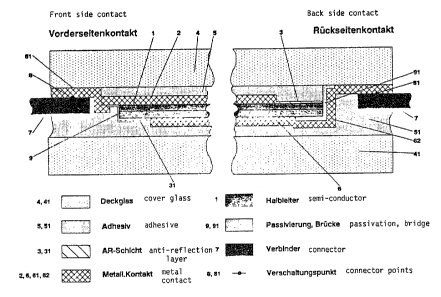
Figure 1 shows a thin solar cell with a semi-conductor body 1
that is of direct semi°conductor material, this preferably being
a gallium arsenide cell that has on its front incident side a
grid-like contact system 2, an anti-reflection layer 3, and a
cover glass 4. The saver glass 9 is secured in place by means of
a temperature-resistant adhesive 5, in order to permit sintering
of the back-side contact 6 to the semi-conductor body 1 should
this be necessary. It is also possible to attach the cover glass
4 by direct fusion (direct glazing). These possibilities for
attachment also apply to the rear cover glass 41.
In order to be able to connect a solar cell connector ? to
produce a series and/or parallel connection of a number of solar


cells to the front and back-side 2 or 6, respectively, on the
side of the adhesive layer 5 or of the cover glass 4,
respectively, that is proximate to the semi-conductor body there
are two connector points 8 and 82 to which the solar cell
connectors 7 are electrically connected and which are connected
so as to be electrically conductive and are cannected to the
front and rear-side contacts 2 and 6 through bridge contacts (see
below). A simple connection between the connector points 8 and
81 and the contacts 2 and 6 thus achieved in that the front side
contact 2 has a connector bar, and in that the back-side contact
6 runs on a face side of the semi-conductor 1 to the cover glass
4, when an insulating layer 91 must be arranged between the face
side of the semi-conductor 1 and the contact piece that is
immediately adjacent thereto (bridge contact s2). More
advantageously, this can be a dielectric 9 that serves to
passivate the face side of the semi-conductor body 1. In the
event, for example, that passivation of the face side should not
be necessary, a bridge through air or a vacuum (an air-bridge
type contact) is also possible.
For all practical purposes, the solar cell described heretofore
is a simple solar cell with a unilateral photo-sensitive surface.
In order to create a bi-facial solar cell with two opposing
photo-sensitive sides, it is first necessary to have an
appropriately suitable epitaxial-layer sequence. Furthermore, a
solar cell of the type shown in figure 1 has a back-side contact
6 that is formed as a grid-like contact system, an anti-
reflection layer 32, and a cover glass 41 that is secured by
means of an adhesive layer 51.
The production of a solar cell as described heretofore is
described on the basis of the drawings 1 to 4 in figure 2, and
figure 1, Initially, a Layer sequence that is useable for a
solar cell is applied to a carrier substrate (semi-conductor body
of semi-conductor material) with the intermediate layers that are
6


needed, depending on the separating process that is used
subsequently. A grid-like contact system 2 with contact bars and
an anti-reflection layer 3, are installed to the front, incident,
side of the semi-conductor body 1 (figure 2, drawing ~,). 'fhe
front, incident, side of the semi-conductor body 1, together with
the contact system 2 and the anti-reflection layer 3 axe then
covered over by a cover glass ~1 (figure 2, drawing 2). Next, the
carrier substrate and any intermediate layers that may be in
place are removed, either wholly or in part, from the semi-
conductor body 1. The four processes described above can be used
to do this. This step in the process is followed, for example,
by an etching process, by means of which the edges, of the semi-
conductor body 1 and simultaneously two sub-areas of the semi-
conductor body 1 are etched off in order to expose a connector
point 8 that is located on the front side contact 2 and to create
a recessed area for the back connecting point 81 (figure 2,
drawing 3). The back-side contact 6 is applied to the back side
of the semi-conductor 1, which has had the carrier substrate and,
if necessary, the intermediate layers removed from it; this back-
side contact 6 extends through the recessed area fox the back-
side connecting point 81, is insulated relative to the face side
of the semi-conductor body ~. (62) as far as the side of the cover
glass 4 that faces the semi-conductor body 1 or as far as an
adhesive layer 5 that is located between cover glass 4 and semi-
conductor body 1, where it forms the connector point 81 for the
back-side contact 6 (figure 2, drawing 4). ~y enlarging 'the
front side contact bar beam, a contact body 61 for the contact
point 8 can be produced directly on the cover glass during
production of the back-side contact 6 of the bridge 61 and of the
contact point 81 on the side of the cover glass that faces the
semi-conductor body (figure l, front side contact). Finally, the
solar connectors 7 are connected to the contact points 8 and 81
that are connected electrically with the front side contact 2 and
with the back-side contact 6.
7


~~'~~,~~"~
It is advantageous that, according to the present invention, both
contact points 8 and 8~. are located on the rear side (solar cell
side) of the cover glass. They can be attached outside, within,
or on the edge of the area that is defined as the solar cell
area. If the contact points are installed on the edges of the
solar cells, it is a simple matter to connect the salar cells to
each other and to do sa with almost no intervening space between
the photoactive surfaces of the cells. There is no additional
loss of active solar cell surface by the contact points 8 of the
front side contacts and the additional loss of active solar cell
area caused by the contact points 81 of the back-side contacts is
very slight and, given a suitable design, can be kept beloT~ 2 per
cent of the total surface area. Positioning the contact. bodies
of the contact points away from the semi-conductor body on the
cover glass or on an intermediate layer, permits firm attachment
of the connectors without any danger of damaging the sensitive
semi-conductor body.
A further advantage of the present invention is the fact that the
edges (solar cell area definition), the opening of the front
connector point and the etching off of a place for the back-side
contact point can be carried out in one step. In addition,
damage to the semi-conductor edge (under-etching, break-through,
etc.) that can possibly occur during a separation process is
eliminated by the etching. Because of the fact that, with
epitaxials, the layers do not grow at the same quality in a strip
of approximately 1 to 2 mm on the edge of the substrate, as is
the case on the semi-conductor (short circuits), at the beginning
of the production process, the substrate must be so selected as
to be greater by this amount than the subsequent photo-
electrically active solar cell area. The present invention makes
use of this fact; during the processing of a complete
epitaxialized wafer to form a single solar cell, this edge strip
that is required for the production of a high quality solar cell
contributes to safe handling, although it is not an essential
8


element of the present invention. Edges that are only a few
microns wide are sufficient.
It is possible that, prior to the installation of the back-side
contact 6, the edges (face sides) of the semi-conductor body 1
that are produced by etching are passivated, for example, by
photo-lacquer, polyimides, nitrides, oxides, by the back-side
anti-reflection layer =bi-facial cell) or other dielectric
materials; this passivation can then also serve as insulation 9
for the bridge contact.
The following, additional process steps are to be carried out for
the production of a bi-facial solar cell:
- a sequence of layers that can be used as a bi-facial solar
cell is to be applied to the carrier substrate;
- a grid-like back-side contact system 6 and an anti-
reflection layer 31 are applied to the rear side from which
the carrier substrate and intermediate layers that may be in
place have been removed;
- a cover glass 41 is applied to the rear side of the solar
cell.
Because of the fact that the front and back-side contact points
are located on one and the same side of the cover glass, it is
very simple to produce a solar cell for both serial and parallel
connection with a special grid design, without modifying either
the process or the grid design, such that 'there is almost no loss
of active surface by connecting these cells to each other and
almost no intermediate space between the active surfaces.
Appropriate examples can be seen from figures 3 to 5.
9

Dessin représentatif
Une figure unique qui représente un dessin illustrant l'invention.
États administratifs

Pour une meilleure compréhension de l'état de la demande ou brevet qui figure sur cette page, la rubrique Mise en garde , et les descriptions de Brevet , États administratifs , Taxes périodiques et Historique des paiements devraient être consultées.

États administratifs

Titre Date
Date de délivrance prévu 2003-08-12
(22) Dépôt 1992-06-19
(41) Mise à la disponibilité du public 1993-04-05
Requête d'examen 1999-03-11
(45) Délivré 2003-08-12
Expiré 2012-06-19

Historique d'abandonnement

Il n'y a pas d'historique d'abandonnement

Historique des paiements

Type de taxes Anniversaire Échéance Montant payé Date payée
Le dépôt d'une demande de brevet 0,00 $ 1992-06-19
Enregistrement de documents 0,00 $ 1993-03-02
Taxe de maintien en état - Demande - nouvelle loi 2 1994-06-20 100,00 $ 1994-05-24
Taxe de maintien en état - Demande - nouvelle loi 3 1995-06-19 100,00 $ 1995-05-19
Taxe de maintien en état - Demande - nouvelle loi 4 1996-06-19 100,00 $ 1996-05-23
Taxe de maintien en état - Demande - nouvelle loi 5 1997-06-19 150,00 $ 1997-05-27
Taxe de maintien en état - Demande - nouvelle loi 6 1998-06-19 150,00 $ 1998-05-20
Requête d'examen 400,00 $ 1999-03-11
Enregistrement de documents 100,00 $ 1999-05-11
Taxe de maintien en état - Demande - nouvelle loi 7 1999-06-21 150,00 $ 1999-06-21
Taxe de maintien en état - Demande - nouvelle loi 8 2000-06-19 150,00 $ 2000-05-24
Taxe de maintien en état - Demande - nouvelle loi 9 2001-06-19 150,00 $ 2001-05-16
Enregistrement de documents 100,00 $ 2001-12-06
Taxe de maintien en état - Demande - nouvelle loi 10 2002-06-19 200,00 $ 2002-05-21
Taxe finale 300,00 $ 2003-05-16
Taxe de maintien en état - Demande - nouvelle loi 11 2003-06-19 200,00 $ 2003-05-21
Enregistrement de documents 100,00 $ 2004-05-12
Taxe de maintien en état - brevet - nouvelle loi 12 2004-06-21 250,00 $ 2004-05-17
Taxe de maintien en état - brevet - nouvelle loi 13 2005-06-20 250,00 $ 2005-05-27
Taxe de maintien en état - brevet - nouvelle loi 14 2006-06-19 250,00 $ 2006-05-24
Taxe de maintien en état - brevet - nouvelle loi 15 2007-06-19 450,00 $ 2007-05-28
Enregistrement de documents 100,00 $ 2007-10-23
Taxe de maintien en état - brevet - nouvelle loi 16 2008-06-19 450,00 $ 2008-05-23
Taxe de maintien en état - brevet - nouvelle loi 17 2009-06-19 450,00 $ 2009-06-04
Taxe de maintien en état - brevet - nouvelle loi 18 2010-06-21 450,00 $ 2010-06-03
Taxe de maintien en état - brevet - nouvelle loi 19 2011-06-20 450,00 $ 2011-06-01
Titulaires au dossier

Les titulaires actuels et antérieures au dossier sont affichés en ordre alphabétique.

Titulaires actuels au dossier
AZUR SPACE SOLAR POWER GMBH
Titulaires antérieures au dossier
ANGEWANDTE SOLARENERGIE - ASE GMBH
BRAUN, MATTHIAS
DAIMLERCHRYSLER AEROSPACE AG.
FRESE, VOLKER
HILGARTH, JUST
RWE SOLAR GMBH
RWE SPACE SOLAR POWER GMBH
TELEFUNKEN SYSTEMTECHNIK GMBH
Les propriétaires antérieurs qui ne figurent pas dans la liste des « Propriétaires au dossier » apparaîtront dans d'autres documents au dossier.
Documents

Pour visionner les fichiers sélectionnés, entrer le code reCAPTCHA :


Pour visualiser une image, cliquer sur un lien dans la colonne description du document. Pour télécharger l'image (les images), cliquer l'une ou plusieurs cases à cocher dans la première colonne et ensuite cliquer sur le bouton "Télécharger sélection en format PDF (archive Zip)" ou le bouton "Télécharger sélection (en un fichier PDF fusionné)".

Liste des documents de brevet publiés et non publiés sur la BDBC .

Si vous avez des difficultés à accéder au contenu, veuillez communiquer avec le Centre de services à la clientèle au 1-866-997-1936, ou envoyer un courriel au Centre de service à la clientèle de l'OPIC.


Description du
Document 
Date
(yyyy-mm-dd) 
Nombre de pages   Taille de l'image (Ko) 
Dessins représentatifs 1998-10-16 1 44
Description 1994-02-26 8 396
Dessins 1994-02-26 3 106
Abrégé 1994-02-26 1 26
Page couverture 2003-07-09 2 74
Page couverture 1994-02-26 1 22
Revendications 1994-02-26 5 216
Revendications 2002-09-03 5 200
Dessins représentatifs 2002-12-05 1 35
Poursuite-Amendment 1999-07-20 1 34
Cession 1999-05-11 15 572
Cession 2004-09-02 2 85
Correspondance 2003-05-16 1 33
Cession 2001-12-06 6 288
Correspondance 2002-02-05 1 11
Poursuite-Amendment 2002-05-02 2 74
Taxes 1999-06-21 1 40
Poursuite-Amendment 2002-09-03 6 232
Cession 1992-06-19 8 294
Poursuite-Amendment 1999-03-11 1 42
Cession 2004-05-12 2 72
Correspondance 2004-06-08 1 26
Cession 2007-10-23 5 148
Taxes 1994-05-24 1 104
Taxes 1995-05-19 1 106
Taxes 1996-05-23 1 132