Note : Les descriptions sont présentées dans la langue officielle dans laquelle elles ont été soumises.
20749~5
A CONSTANT IMPEDANCE TRANSITION BETWEEN
TRANSMISSION STRUCTURES OF DIFFERENT DIMENSIONS
BACKGROUND OF THE INVENTION
The disclosed invention is directed generally to
hybrid multilayer circuit structures, and is directed more
s particularly to connected microstrip transmission lines of
different dimensions disposed on hybrid multilayer circuit
structures and having a substantially constant impedance.
Hybrid multilayer circuit structures, also known as
hybrid microcircuits, implement the interconnection and
packaging of circuit devices (e.g., integrated circuits),
and generally include a unitized multilayer circuit struc-
ture formed from a plurality of integrally fused insulating
layers (e.g., ceramic layers) having conductor traces
disposed therebetween. The circuit devices are commonly
mounted on the top insulating layer so as not to be covered
by another insulating layer or on an insulating layer
having die cutouts formed thereon to provide cavities for
the circuit devices. Passive components such as capacitors
and resistors can be formed on the same layer that supports
the circuit devices, for example, by thick film processes,
or they can be formed between the insulating layers, for
example, also by thick film processes. Electrical inter-
connection of the conductors and components on the differ-
ent layers is achieved with vias or holes appropriately
located and formed in the insulating layers and filled with
~L,
-
~719~
conductive via fill material, whereby the conductive
material is in contact with predetermined conductive traces
between the layers hat extend over or under the vias.
Hybrid multilayer circuit structures are now being
utilized for RF applications wherein microwave integrated
circuits (MICs) and/or monolithic microwave integrated
circuits (MMICs) mounted on a hybrid are interconnected by
microstrip transmission structures formed on the multilayer
structure, for example pursuant to screen printing or metal
deposition.
A consideration with implementing microstrip transmis-
sion structures in hybrid multilayer circuit structures is
the desirability of reducing signal reflection at the
transitions between microstrip lines of different widths,
where a variable width is being utilized for considerations
such as reducing loss, layout requirements and processing
requirements.
SUMMARY OF THE INVENTION
It would therefore be an advantage to provide low-
reflection transitions between transmission structures of
different dimensions.
The foregoing and other advantages are provided by the
invention in a transmission line structure having a sub-
stantially constant characteristic impedance along its
length so that reflections due to impedance change are
negligible, whereby the total signal reflection is reduced.
An illustrative embodiment of a microstrip transmission
line structure in accordance with the invention includes a
series of connected microstrip strip sections having
different widths forming a microstrip line on the top layer
of a unitized multilayer circuit structure, respective
ground planes for each of said strip sections formed
between insulating layers of the multilayer circuit struc-
2~4~S
ture respectively dielectrically spaced from the associated
strip sections to provide a substantially constant imped-
ance along the length of the microstrip line, and a plural-
ity of conductive vias for electrically interconnecting the
respective ground planes.
BRIEF DESCRIPTION OF THE DRAWINGS
The advantages and features of the disclosed invention
will readily be appreciated by persons skilled in the art
from the following detailed description when read in
conjunction with the drawing wherein:
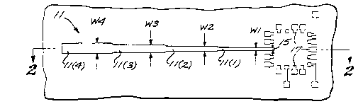
FIG. 1 is a top plan view of a portion of a unitized
multilayer circuit structure in which is implemented a
microstrip transmission line structure in accordance with
the invention.
FIG. 2 is a sectional view illustrating the stepped
ground planes of the microstrip transmission line structure
of FIG. 1.
FIG. 3 is a sectional view illustrating a further
stepped ground plane structure for the microstrip line of
FIG. 1.
FIG. 4 is a top plan view of a curved microstrip
section that can be utilized in the microstrip transmission
line of the invention.
FIG. 5 is a top plan view of a microstrip section with
a bend that can be utilized in the microstrip transmission
line of the invention.
DETAILED DESCRIPTION OF THE DISCLOSURE
In the following detailed description and in the
several figures of the drawing, like elements are identi-
fied with like reference numerals.
~U7~
A microstrip transmission line structure in accordance
with the invention is implemented in a unitized multilayer
circuit structure that is utilized for interconnecting
various circuit devices such as MICs and/or MMICs mounted
on the outside of the unitized structure. The unitized
multilayer circuit structure is formed from a plurality of
insulating layers (comprising ceramic, for example),
conductive traces disposed between the layers and on the
top layer (including for example microstrip lines), and
conductive vias formed in the layers which together with
any buried elements (e.g., elements formed on the top of an
insulating layer and covered by an overlying insulating
layer) are processed to form an integrally fused unitized
multilayer structure. After the unitizing fabrication,
appropriate metallization is applied to the outside of the
unitized structure, and the circuit devices are mounted and
electrically connected.
Referring now to FIGS. 1 and 2, set forth therein is
a top plan view and an elevational sectional view of a
microstrip transmission line structure that includes a
stepped microstrip line 11 disposed on the top layer of the
multilayer circuit structure with which the transmission
line structure is implemented. The microstrip line 11
includes a series of interconnected strip sections of
respective fixed widths. Each fixed width strip section
can comprise, for example, a linear strip section, a curved
strip section or a section containing a bend.
For ease of illustration and explanation, the specific
example will be discussed of a stepped microstrip line
having fixed width linear strip sections 11(1), 11(2),
11(3) 11(4) of different fixed widths Wl, W2, W3, W4. The
widths of the linear strip sections increase from right to
left, and by way of example, the narrowest strip section
11(1) is connected to a chip bonding pad 15 that is of
about the same width as the strip section 11(1). Further
~U749~5
chip bonding pads 17 together with the chip bonding pad 15
can be utilized for connection to a MMIC, for example.
The microstrip transmission line structure further
includes embedded ground plane metallization layers 13(1),
13(2), 13(3), 13(4) formed between different insulating
layers and respectively associated with the different
segments of the microstrip line, with the ground plane
spacing being greater for greater strip section width.
Each ground plane is at a fixed spacing relative to its
associated strip section, with no intervening ground planes
or conductive elements between a strip section and the
portion of its associated ground plane that is directly
beneath the strip section. The strip section widths and
associated ground plane spacings are selected to provide
for the same characteristic impedance for all of the strip
sections, which provides a substantially constant impedance
along the length of the line. To the extent that the
bonding pad lS is an extension of the strip section 11(1),
the associated ground plane 13(1) should extend beneath the
bonding pad 15.
For the illustrative example of having a MMIC bonded
to the bonding pads lS, 17, the embedded ground planes
should not extend to areas beneath the area enclosed by the
bonding pads, so as to minimize the effect on the perfor-
mance of the MMIC.
Since the ground plane spacings are constrained to be
integral multiples of the thickness of each of the layers
of the multilayer circuit structure, the specific line
widths are dependent upon the ground plane spacings. In
terms of implementation, an initial approximation for a
particular strip section width would be utilized to deter-
mine a specific ground plane location, which in turn would
define the specific line width that would need to be
utilized, given a particular dielectric constant.
~074~
The ground planes are stepped such that the each of
the ground planes extends beneath overlying ground planes
to one end of the microstrip line, and the lowermost ground
plane extends the entire length of the microstrip transmis-
sion line. The embedded ground planes are electricallyinterconnected by conductive vias 14, and the interconnect-
ed embedded ground plane structure is electrically connect-
ed by columns of conductive vias 16 to a bottom ground
plane 213 formed on the lower surface of the unitized
multilayer circuit structure in which the microstrip
transmission line structure is implemented. Each column
can comprise axially aligned vias or staggered vias which
are interconnected with conductor traces or catch pads, as
for example disclosed in commonly assigned U.S. Patent
4,899,118, February 6, 1990, incorporated herein by refer-
ence. Whether axially aligned vias or staggered vias are
utilized depends on factors such as those affecting the
electrical, thermal, or mechanical integrity of the unit-
ized multilayer circuit structure. It should be appreciat-
ed that a generous amount of conductive vias has been
utilized and arranged in parallel so as to reduce the
inductive effects of the vias.
While the lowest ground plane of the stepped micro-
strip transmission line structure has been shown as an
embedded ground plane, such lowest ground plane can com-
prise the bottom ground plane of the multilayer circuit
structure, depending upon factors such as the width of the
widest strip section widths and the number of layers in the
unitized multilayer circuit structure.
Referring now to FIG. 3, set forth therein is a
further embodiment of a microstrip transmission line
structure in accordance with the invention configuration
wherein the ground planes 113(1), 113(2), ... 113(4) extend
only slightly beneath an immediately overlying embedded
ground plane. The embedded ground planes are electrically
207~97~
connected to each other and to a bottom ground plane 213 by
conductive vias 114 which can be arranged in columns for
connections that extend through more than one insulating
layer. Each column of conductive vias can comprise axially
aligned vias or staggered vias which are interconnected
with conductor traces or catch pads, as discussed above
relative to the structure of FIG. 2. It should be appreci-
ated that a generous amount of conductive vias should be
utilized and arranged in parallel so as to reduce the
inductive effects of the vias. As with the structure of
FIG. 2, the structure of FIG. 3 can include the bottom
ground plane as the lower most ground plane for the widest
strip section.
A consideration in utilizing the ground plane struc-
ture of FIG. 2 is better continuity and less inductance
between ground planes, while a consideration in utilizing
the ground plane structure of FIG. 3 is less metal between
the layers which provides for better adhesion between the
layers of the unitized multilayer circuit structure.
For purposes of schematic illustration the embedded
ground planes are shown as being between contiguous layers,
based on the illustrative example that the change in width
between contiguous strip sections requires a change in
spacing the corresponds to the thickness of one insulating
layer. However, the actual spacing depends on the widths
of the respective strip sections which are constrained to
be at discrete values as determined by the available ground
plane depths that are constrained to be integral multiples
of layer thickness. Further, depending upon particular
requirements, the widths of the strip sections do not have
to be all increasing or decreasing in a given direction
along the length of the microstrip transmission line.
Also, the transition in strip section width does not have
to be gradual and the individual changes in width can be
relatively large.
207497~
Referring now to FIGS. 4 and 5, set forth therein are
an example of a constant width curved strip section 211 of
constant width and an example of a constant width strip
section 311 with a bend, which can be utilized in the
microstrip transmission line structure in accordance with
the invention.
The widths of the ground planes as measured laterally
relative to the centerline of the associated strip section
line will depend upon the particular application and the
possible layout constraints. For example, a ground plane
width that is about 3 to 5 times the width of the associat-
ed strip section would be appropriate for most cases to
avoid finite ground plane effects. If finite ground plane
effects cannot be avoided, they can be appropriately
compensated. It should be appreciated that the desired
width for a ground plane ground plane for a curved section
or a section having a bend should be satisfied at all
points along the length of the strip section.
Pursuant to the transmission line structure of the
invention, a substantially constant impedance path is
provided between connected strip sections of different
widths, which can be advantageously utilized in applica-
tions that require a change in microstrip line width, such
as connection of a microstrip line of predetermined width
to a narrower chip bonding pad 15 as shown in FIG. 1.
Microstrip transmission line structures in accordance
with the invention are made, for example, pursuant to low
temperature co-fired processing such as disclosed in
"Development of a Low Temperature Co-fired Multilayer
Ceramic Technology," by William A. Vitriol et al., 1983
ISHM Proceedings, pages 593-598; "Processing and Reliabili-
ty of Resistors Incorporated Within Low Temperature Co-
fired Ceramic Structures," by Ramona G. Pond et al., 1986
ISHM Proceedings, pages 461-472; and "Low Temperature Co-
2~7~975
Fireable Ceramics with Co-Fired Resistors," by H.T. Sawhill
et al., 1986 ISHM Proceedings, pages 268-271.
In accordance with low temperature co-fired process-
ing, vias are formed in a plurality of green thick film
tape layers at locations defined by the desired via config-
urations of the desired multilayer circuit. The vias are
filled with the appropriate fill material, for example, by
screen printing. Conductor metallization for conductive
traces including the embedded ground planes are then
deposited on the individual tape layers by screen printing,
for example, and materials for forming passive components
are deposited on the tape layers. The tape layers are
laminated and fired at a temperature below 1200 degrees
Celsius (typically 850 degrees Celsius) for a predetermined
length of time which drives off organic materials contained
in the green ceramic tape and forms a solid ceramic sub-
strate. External metallization including the microstrip
sections of different widths, a lower ground plane metall-
ization and any side wall metallization can then be applied
by known techniques.
Although the foregoing has been a description and
illustration of specific embodiments of the invention,
various modifications and changes thereto can be made by
persons skilled in the art without departing from the scope
and spirit of the invention as defined by the following
claims.