Note : Les descriptions sont présentées dans la langue officielle dans laquelle elles ont été soumises.
2~'82~53
POWER CONVERSION SYSTEM
Background of the Invention
Field of the Invention
The invention relates to a power conversion system
in which a line-commutated power conversion system and a
self-commutated power conversion system are coupled.
Description of the Related Art
Line-commutated power conversion systems are widely
used for conversion from AC power to DC power or from DC
power to AC power. By way of example, large-scale systems
are used in power conversion systems for DC power
transmission.
However, large-scale line-commutated power conversion
systems require LC filters consisting of a reactor and a
capacitor in order to reduce harmonics and compensate
lagging reactive power, but in addition to the problem
that the space required for the LC filter is large, there
are problems of overcurrent in the LC filter caused by
ingress of harmonics from the outside and the occurrence
of antiresonance caused by the LC filter and the reactance
of the system.
Further, in line-commutated conversion systems, a
switching device is commutated using the system voltage
so that there is also a problem in that commutation
failure is caused and the system damaged if the voltage
of the system should drop or voltage distortion occur
during inverter operation.
Active filters and reactive power adjusting devices
using voltage type self-commutated power conversion
systems instead of LC filters have recently appeared
- 2082S53
together with advances in self-¢ommutated power
conversion technology.
By way of examples, active filters _nd re_ctive power
adjusting devices, products classed from sever_l NVA to
sever_l tens of NVA have been produced starting with the
device disclosed in the "Toshiba Review" ~Vol. 43, No. 4,
pp. 339 to 342) for example. The power conversion
circuit is of the voltage type self-commutated type. The
primary problem in systems using thi~ voltage type self-
commutated power convorsion system is overcurrent
protection in the switching device during a DC short-
circuit.
The problQms associated with a main circuit become
particularly apparent _t higher c_pacities. To
elabor_te, should the GTO (G_te Turn-Off) thyristors be
ON at the same time due to a control irregul_rity or the
like, the charge of the DC capacitor is dischargQd
through the GTo thyristors. If there is a rapid rise in
the short-circuit current it is impossible to use the
current circuit-brea~;ng function of the GTO thyristor at
this time _nd there is a risk of overcurrent bre_kdown of
the GTO thyristor. Protective fuses _re inserted to
prevent the risk.
However, protective fuses are not av_ilable for
higher voltages ~nd some customers do not like to use
them for re_sons of gu_r_nteeing long-term reliability,
and there is a demand for devices to replace them.
8umm_ry of the Invention
It is therefore an object of the invention to provide
_ power conversion system comprising a line-commutated
power converter and a self-commutated power converter,
wherein their respective strengths can be made use of and
their respective wea~ne~ses can be complemented by each
other.
To achieve the above object, a power conversion
system comprising line-commutated power converting means
~n~5~
in which a line-commutated power conversion circuit and a
coupling diode are coupled to form a DC circuit and for
converting DC power into AC power or AC power into DC power,
and self-commutated power converting means in which a self-
commutated power conversion circuit is coupled to the coupling
diode in order to form a DC circuit and for reducing reactive
power, or the reactive power and harmonics generated by the
line-commutated converting means.
According to the above-structured power conversion
system of the invention, the line-commutated power converting
means governs the power conversion from DC power to AC power
or from AC power to DC power and the self-commutated power
converting means reduces the reactive power, or the reactive
power and harmonics generated by the line-commutated power
converting means, and both operate more or less independently,
but during the rare direct current short-circuiting of the
self-commutated power converting means, conduction by said
coupling diode is blocked so that the line-commutated power
converting means and the self-commutated power converting
means operate in series. Thus the overcurrent in the self-
commutated power converting means side is limited by the
constant current control function of the line-commutated power
converting means and the short-through is safely removed by
the turn-off action of the switching devices by the intrinsic
circuit-breaking function. This makes it possible to make
self-commutated power converting means fuseless and smaller in
scale.
28516-5
5 !5 3
-3a-
In accordance with the present invention, there is
provided a power conversion system comprising line-commutated
power converting means for converting from DC power to AC
power or from AC power to DC power; self-commutated power
converting means for reducing reactive power by the line-
commutated power converting means; and a coupling means for
forming a first closed circuit with the line-commutated power
converting means and a second closed circuit with the self-
commutated power converting means, wherein the line-commutated
power converting means comprises a circuit breaker, a trans-
former, a reverse-conducting bridge connected power converter,
a reactor and a DC capacitor, the coupling means is a diode,
the first closed circuit comprises a load, the diode, the DC
reactor, and the reverse-blocking bridge connected power
converter, and the second closed circuit comprises the DC
capacitor, the diode, and the reverse-conducting bridge
connected power converter.
In accordance with the present invention, there is
further provided a power conversion system comprising line-
commutated power converting means for converting from DC powerto AC power or from AC power to DC power; self-commutated
power converting means for reducing reactive power by the
line-commutated power converting means; and a coupling means
for forming a first closed circuit with the line-commutated
power converting means and a second closed circuit with the
self-commutated power converting means, wherein the line-
commutated power converting means comprises a circuit breaker,
28516-5
-3b-
a transformer, a reverse-blocking bridge connected power
converter, and a DC reactor, the self-commutated power
converting means comprises a circuit breaker, a transformer, a
reverse-conducting bridge connected power converter, a reactor
and a DC capacitor, the coupling means is a diode, the first
closed circuit comprises a DC power source, the diode, the DC
reactor, and the reverse-blocking bridge connected power
converter, and the second closed circuit comprises a DC power
source, the diode, and the reverse-conducting bridge connected
power converter.
In accordance with the present invention, there is
further provided a power conversion system comprising a pair
of self-commutated power converters having AC terminals which
are respectively connected to a first AC system and a second
AC system and DC terminals, and being provided in common with
a series circuit comprising a DC capacitor between the DC
terminals and a coupling diode inserted with polarity such as
to block the discharge current of the DC capacitor; and a pair
of line-commutated power converters that perform line-
commutated commutation, having AC terminals being respectivelyconnected to the first AC system and second AC system, and
which are connected such that the coupling diode is contained
in series and such that DC current flows through the coupling
diode.
In accordance with the present invention, there is
further provided a power conversion system comprising a pair
of voltage type self-commutated converters that perform self-
r~ 28516-5
commutated commutation and have AC terminals being respect-
ively connected to a first AC system and a second AC system
and DC terminals, one end of a DC capacitor being connected to
one end of the DC terminals of a coupling diode bridge, the
other end of the coupling diode bridge being connected as DC
terminals; and a pair of line-commutated converters that
perform line-commutated commutation, have AC terminals being
respectively connected to the first AC system and the second
AC system, and are connected such that DC circuits are formed
through the DC terminals of the coupling diode bridge and such
that their DC currents flow through the coupling diode bridge.
Brief Description of the Drawinqs
Fig. 1 is a diagram of a power conversion system
illustrating first embodiment of the invention;
Fig. 2 is a diagram illustrating one example of a
reverse blocking type bridge connected converter;
28516-5
_ -4- 2~825~3
Fig. 3 is a diagram showing paths along which current
flows during DC short-circuiting of the reverse
conducting type bridge connected converter;
Fig. ~ is ~ diagram illustrating one ex~mple of a
reverse conducting type bridge connected converter;
Fig. 5 is a diagram of a power conversion system
illustrating second embodiment of the invention;
Fig. 6 is a diagram of a power conversion system
illustrating third embodiment of the invention;
Fig. 7 is a diagram of a power conversion system
illustrating fourth emboaiment of the invention;
Fig. 8 is a ~iagram of a power conversion system
illustrating fifth embodiment of the invention;
Fig. 9 i~ ~ diagram of ~ power conversion system
illustrating sixth embodiment of the invention;
Fig. 10 is a diagram of a power conversion system
illustrating seventh emboaiment of the invention;
Fig. 11 is a diagram of a power conversion system
illustrating eighth embodiment of the invention
Fig. 12 is a diagr~m showing paths along which
current flows during DC short-circuiting of a reverse
conaucting type bridge connected converter of the eighth
embodiment in Fig. 11;
Fig. 13 i8 a diagram of a power conversion system
illustrating ninth embodiment of the invention;
Fig. 14 is a aiagram of a power conversion system
illustrating tenth embodiment of the invention;
Fig. 15 is a diagram of a power conversion system
illustrating eleventh embodiment of the invention.
Detailed Description of the Preferrea Embodiments
Preferred embodiments of the invention will now be
describea referring to the accompanying drawings.
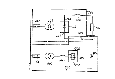
As shown in Fig. 1, a power conversion system of a
first embodiment comprises a line-commutated power
conversion apparatus 100 and a voltage type self-
commutated power conversion apparatus 200. Both
~~5~ ~n82553
apparatus 100 and 200 are coupled by a eoupling diode
107.
The line-commutated power eonver~ion apparatus
comprises a circuit breaker 101, a transformer 102, a
reverse bloe~; n7 type bridge eonnected power eonverter
103 having a positive terminal 104 and a negative
terminal 105, a DC reaetor 106 and the eoupling diode
107.
Also the voltage type self-eommutated power
10eonver~ion apparatus 200 eomprises a eireuit breaker 201,
a tran~former 202, a eoupling reaetor 203, a reverse
eondueting type bridge eonneeted power eonverter 204
having a positive terminal 205 and a negative terminal
206, a DC eapaeitor 207 and the eoupling diode 107.
15Further, the reverse bloeking type bridge eonneeted
power eonverter 103 may be a thyristor rectifier as shown
in Fig. 2.
As the eoupling diode 107 is eonneeted in the
direetion of DC eurrent flow, the normal operation of the
line-eommutated power eonver~ion apparatus 100 is not
influeneed by the eoupling diode 107.
on the other hand as the eoupling diode 107 is
inserted with the polarity in Fig. 1 in the voltage type
self-eommutated power conversion apparatus 200, the
capacitor 207 is charged but there is no pathway for
diseharging in the voltage type self-eommutated power
eonversion apparatus 200.
Consequently the voltage type ~elf-commutated power
eonversion apparatus 200 does not operate alone.
However, if the line-eommutated power eonversion
apparatus 100 is operated and a current Il flows in the
coupling diode 107, th~ voltage type ~elf-eommutated
power eonversion apparatus 200 operates in exactly the
same way as when there is no coupling diode provided that
the eurrent in the diseharge direetion flowing in the DC
eapaeitor 207 is less than the eurrent Il.
However, if for some reason the reverse eondueting
type bridge eonneeted power eonverter 204 suffer~
_ -6- ~0825~3
commutation failure, the terminals 205 and 206 ~re short-
circuited, and the charge of the capacitor 207 attempts
to flow through the short-circuit path. Further if this
value is about to ~Ycee~ the current Il, the current in
the coupling diode 107 is zero and the coupling diode 107
enters the reverse blocking state.
As result, a~ shown in Fig. 3, the discharge current
Ic flows through the circuit of the line-commutated power
conversion apparatus 100 and the increase in current is
restricted. 8ubsequently, a protective operation is
¢arried out by a signal from a commutation failure
detection circuit ~not shown). The co lutation failure
detection ¢ircuit protects the power conversion ~ystem
from the overcurrent caused by the commutation failure.
Further, a choice is made depending on the cause of the
commutation failure as to whether to restart the
operation or to ~top the voltage-type self-commutated
power conversion apparatus 200 and only operate the line-
commutated power conversion system 100, 80 preventing a
drop in the wor~ing efficiency of the power conversion
system.
Now the operation of protecting the reverse
conducting type bridge connected power converter 204 will
be described.
Referred to Fig. 4, the GTO thyristors 211, 214 and
216 are fired, currents Iu, Iv and Iw flow into terminals
U, V and W respectively. If curront Iw is flowing, and
the GTO thyristor 215 is fired by accident, a DC short-
circuit occurs between the GTO thyristor 215 and the GTO
thyristor 216.
As described above, as the current Il flows through
the point of short-circuit, the current I1 flows into the
GTO thyristor 215 and the currents Iw and Il flow into
the GTO thyristor 216. If the maximum current value at
which the GTO thyristor can be turned off by its gate is
In~ and the value of current Iw plus current Il is equal
to I~ or less, the GTO thyristor can be provided with
an OFF signal and can be turned off safely. However, if
7- 2~82~53
the value of current Iw plus current I1 i~ more th_n the
I~ and the GTO thyristor is provided with the CFF
signal, it will be dQstroyed due to overcurrent.
Accordingly, for safe operation, the current Il must
satisfy the following expression.
Iw I Il < I~
Consequently, if the GTO thyristors 215 _nd 216 are
turned off, the short-circuit iq removed. The GTO
thyri~tor 216 can then also be turned off safely and the
system can be restarted immediately.
A method of providing ON signal to other GTO
thyristors of pha~es which did not ~hort-circuit at the
s~me time after detecting the ~hort-circuited condition
as a method of decreasing current value flowing in a
~hort-circuited portion.
Next _ second embodiment will be de~cribed with
reference to Fig. 5.
As shown in Fig. 5, in this embodiment a DC power
source 120 has been connecte~ instead of the load. The
line-commut~ted power conversion apparatus 100 freely
converts from AC to DC and from DC to AC by changing the
firing control angle of the thyristor.
Next a third embodiment will be dQscribed with
reference to Fig. 6.
A voltage type self-commutated power conversion
apparatus in Fig. 6 also has the function of reducing
harmonics a8 well a8 the function of adjusting reactive
power while supplying active power to the system by
converting DC power to AC power.
The power conversion system shown in Fig. 1, Fig. S
and Fig. 6 have various other ~lternative~. The
embodiment~ ~hown below illu~trate alternatives of the
power conversion system in Fig. 1, but similar
alternatives are also pos~ible for the power conversion
systems in Fig. 5 and Fig. 6.
Fig. 7 show~ a fourth embodiment of the invention.
This embodiment shows that the position where the
-8- 2082~53
coupling diode 107 is inserted can be varied freely in
the clo~ed circuit constituted by the rever~e blocking
type bridge connected power converter 103, DC reactor
106, load 110, and the coupling diode 107 in the power
conver~ion systQm in Fig. 1. It also shows that the
function of coupling reactor 203 is included in the
leakage reactance of tran~former 208 and the function of
circuit breaker 201 is included in the circuit breaker
101 .
Also in this system the transformer 208 is connected
to the DC winding side of the tran~former 102. This
allows the freguency of occurrence of commutation failure
in the line-commutated power conversion apparatus to be
reduced as far as possible by preventing the ~ystem
voltage from falling due to reactive power supplied by
the voltage type self-commutated power conversion
apparatus and reducing the distortion of the system
voltage by a harmonic reducing function. However in this
case lea~age reactance of transformer is set at low
level. Of course, it i8 po~sible to reduce the freguency
of commutation failure and the like as well, but this
depen~ on the sises and proportions of the impedance of
the tran~former 102 and the impe~Ancq on the system side.
Large capacity system~ require duplication of the
reverse conducting type bridge connected power converter
204. A fifth embodiment through a ~eventh embodiment are
shown in Fig. 8 to Fig. 10.
In the fifth embodiment in Fig. 8, two coupling
diodes 107 are inserted in seriQs, and series circuits
consisting of reverse conducting type bridge connected
power converters 2041 and 2042 and DC capacitor~ 2071 and
2072 are connected to these with the polarity depicted.
Waveform synthesis with a tran~former 209 using two
reverse conducting type bridge connected converters in
this way i8 a technigue g~nerally widely usQd for
duplicate inverters. Even if one of the reverse
conducting type bridge connected power converters 2041 or
2042, or both, cau~es a DC short circuit, the conduction
9 20~553
of one or both of the coupling diode~ 1071 or 1072 is
bloc~ed as in Fig. 1, the line-commutated power
conversion apparatus 100 and the voltage type self-
commutated power conversion apparatus 200 are connected
in series and it proves possible to move the protection
operation while the rise in the ~hort circuit current is
limited.
In the sixth embodiment in Fig. 9, the positional
relationship between the DC capacitor 207 and the reverse
conducting type bridge connecter power converter 204 has
been reversed. Coupling reactor 203 may be inserted on
the AC winding sidQ of the transformer as in Fig. 9, or
it can be inserted in the DC w;n~;ng side as in Fig. 1,
or omitted if a high-impedance transformer is used.
lS In the sQventh embodiment in Fig. 10 is a format
effective in large capacity power conversion systems a~
in Fig. 8: a plurality of serial circuits consisting of
a DC reactor 106 and coupling diode 107 are connected in
parallel, and reverse conducting type bridge connected
power converters 204 and DC capacitors 207 are connected
to the coupling diodes. In this case too, the DC
capacitors may be divided as in Fig. 8 and Fig. 9.
The insulating transformers 102, 202 and 209 in the
embodiments in Fig. 1 to Fig. 10 are used normally when
connected to the system. It i8 clear that there is no
need to provide insulating transformers in both the line-
commutated power conversion apparatus 100 and the voltage
type self-commutated power conversion apparatu~ 200
although, in principle, the AC side must be insulated
since the two apparatu~ are coupled by the coupling diode
107 in the direct current portion.
Example~ have been given in the preceding ~escription
in which the voltage type self-commutated power
conversion apparatus has been used as a reactive power
adjusting device, active filter or invertor, but it is
clear that in principle it can also be used to convert
from AC power to DC power. In addition to the device
commutation power converter shown in Fig. 4, a converter
20825~3
using impulse eommutation type or another type self-
commutated power eonversion apparatus can be
appropriately used as the reverse eon~ucting type bridge
eonnected power converter.
Next an eighth embodiment of this invention will be
described with referenee to Fig. 11.
A power conversion system of thi~ embodiment as shown
in Fig. 11 eompri~e~ a fir~t AC line 300a, a sQeond AC
line 300b, ~ line-commutated power conversion apparatus
400, a self-commutated power convQrsion apparatus 500.
The interiors of line-eommutated power conversion
apparatus 400 and ~elf-eommutated power eonversion
apparatus 500 are symmetrieal a~ between the ~ide
a~soeiated with AC line 300a and the side assoeiatQd with
AC line 300b. The referenee numerals of the eonstituent
devieQs are therefore distinguished by the suffixes a and
b.
The power souree terminals of eireuit breakers 401
and 501 are respeetively eonneeted to AC lines 300a and
300b. The load terminal of eireuit breaker 401 i8
eonneeted to the input terminal of a transformer 402 and
the load terminal of eireuit breaker 501 is eonneeted to
the input terminal of a transformer 501.
The output terminal of transformer 402 is eonneeted
to the AC terminal of a reverse bloç~;~g type bridge
eonneeted power converter 403 while the output terminal
of transformer 502 is eonnected to the AC terminal of a
rever~e conducting type bridge eonnected power converter
504 through a reactor 503.
The reverse bloc~;ng type bridge connected power
eonverter ~03 has a positive eleetrode terminal 404 and
a negative eleetrode terminal 405.
The negative electrode terminal 405 and one end of
reactor 406 are connected. The positive electrode
terminal 404 and the anode of a coupling diode 407 are
eonneeted. The po~itive eleetrode terminal 404 is
eonneeted to the other end of reaetor 406. The eathode
of eoupling diode 407 is eonneeted to the negative
2~i~2~3
electrode terminal 405 of reverse blor~tng type bridge
connected power converter 403, forming a pair.
A sQries circuit consisting of a DC cap_citor 507 and
coupling diode 407 i~ connected between positive
electrode terminal 505 and negative electrode terminal
506 of reverse conducting type bridge connected power
converter 504 with _ polarity ~uch _~ to bloc~ di~ch_rge
of DC cap_citor 507.
The oper_tions of the line-commut_ted power
conversion apparatus 400 and 8elf-commutated power
conversion apparatus 500 are the same a~ the opQrations
described in the first embodiment. Con~equently the
operations are not described in this embodiment in
detail.
15Howover, if for ~ome reason there is a f_ilure of
commut_tion of the reverse conducting type bridge
connected power converter 504a on the sidQ of AC line
300_, when terminal~ 505_ _nd 506_ go into a ~hort-
circuited condition, the di~charge current of DC
20capacitor 507 trie~ to flow through the ~hort-circuit
with the result that its value tries to exceed Il.
However, when thi~ happen~, the current of coupling diode
407 goe~ to zero, 80 that ¢oupling diode 407 goes into _
bloc~ing condition.
25A~ _ re~ult, a8 shown in Fig. 13, in which identical
parts to those of Fig. 11 are given the ~_me reference
numerals, discharge current Ic flow~ through the circuit
of line-commutated power conversion apparatu~ 400 which
~uppresses thi~ di~charge current Ic to Il. The GTO
30thyri~tor of the healthy reverse conducting type bridge
connected power converter 504b i8 therefore turned off by
_ sign_l gener_ted by a commut_tion f_ilure detection
circuit (not shown). An OFF sign_l i~ ~imultaneou~ly
supplied to the GTO thyristor of the faulty reverse
35conducting type bridge connected power converter 504_.
The difference between thi~ embodiment _nd the
embodiment de~cribed in Fig. 1 is a current value flowing
in the short-circuit portion.
-12- 2082553
Though the eurrent value is the value I1 ~ Im in the
embodiment deseribed in Fig. 1, the eurrent value in this
embodiment i~ the value Il ~ Im ~ I~. NOW I~ means a
direct eurrent flowing the reverse conducting type bridge
eonneeted power eonverter 504b.
Con~equently the eurrent value deseribed in thi~
embodiment ha~ two eases due to the direction of flowing
of the direet eurrent. One i8 that the curront value i8
larger than the value Il + I~ and the other is that it is
lower than the value Il ~ Im-
It may be seleeted whether the operation of rever~e
eondueting type bridge eonnected power eonverter 504b
stop or not at the same time to short-eireuit in order to
deerease the eurrent flowing at the short-eireuit portion
as large as possible.
Also in ease of Fig. 11, it is effeetive to turn on
all of GTO thyristors in the reverse eondueting type
bridge eonneeted power eonverter whieh short-eireuited
and to disperse the short-eireuit eurrent.
The Fig. 13 i8 a diagram showing a ninth embodiment
of thi~ invention. The differenee from Fig. 11 lies in
that a single-phase diode bridge 410 is employed for
eoupling instead of eoupling diode 407. The single-phase
diode bridge ~10 has DC terminals 411 and 412 and AC
2 5 terminal~ 413 and 414. Ordinary operation in this ease
is the same a~ in Fig. 11.
Considering the ease where short-eireuit oeeur~ in
the ux pole of reverse eonducting bridge connected
eonverter 504a as in Fig. 11, entry of the DC eurrent I~
of reverse eondueting type bridge eonneeted power
eonverter 504b is bloeked by single-phase diode bridge
410, ~o the GTO thyristor eurrent of the ux pole beeome~
Iu, ~ Il while the other GTO thyristor eurrents are Il. If
a seleetive turn-off proeedure i~ adopted 80 long a~
I~ ~ Il, Il ean be bigger than in Fig. 11. Now the ux
pole means the portion eonstituted in the bridge
eonneeted eireuit of Fig. 4 by GTO thyristors 211 and
-13- ~8~5~
212, diode~ 217 and 218 and fuReR 223 and 224, and formR
one pha~e.
Fig. 1~ ~how~ yet a tenth embodiment of thi~
invention. In thi~ embodiment, two ~elf-commutated power
conver~ion apparatu_ a~ in Fig. 11 are provided.
Further, in thi~ embodiment, eoupling reaetor 503a
and tran~former 502a are integrated and substituted by
high-induetanee tran_former~ 508. The primary winding~
of two high-induetanee transformers 508 are eonneeted in
_erie~. Voltage eompo~ition u~ing a tran~former i8 often
carried out, in order to reduce waveform distort~on on
the AC side of a plurality of reverRe eonducting type
bridge eonnected power eonverter~ 504 in a voltage type
~elf-commutated power eonverter.
Cireuit-breaker 501a i~ eonnected to the ~eeondary
~ide of transformer 402a of line-commutated power
conversion apparatu~ 400. A reaetor 408 is in~erted
between thi~ ~eeondary side and reverse bloeking type
bridge eonneeted power eonverter 403a. Thi~ i~ provided
with the aim of deerea~ing outflow of higher harmonic
current to the sy~tem and reducing the frequency of
commutation failure of reverse bloeking type bridge
connected power converter 403a, by reducing the voltage
drop generated in AC line 300a and the higher harmonic~
generated by reverse blocking bridge eonnqcted converter
403a in self-commut~ted power conver~ion apparatu~ S00.
Fig. 15 ~how~ an eleventh emho~;ment in which two
~elf-commutated coupling RyRtem~ as in Fig. 13 are
employed. In this caRe alRo, the primarie~ of
tran~former~ 502 are connected in ~eries.
In the above de~cription, GTO thyri_tors are employed
as rever~e conducting type bridge connected power
converter 50~, but other devices could al~o be u~ed.
Furthermore, apart from device-commutated power
converter~, impul~e commutation or another Relf-
commutated commutation type power eonverter could be
employed.
-14- 20~2~3
In the embodiments of Fig. 11 to Fig. 15, the
coupling diode or switching device was shown by a single
symbol, but these could be appropriately used in series
or in p~r~llel depending on the voltage or current.
As described above, according to the eighth
embodiment through the eleventh embodiment, the self-
commutated power conversion apparatus reduces the
reactive power and generation of higher harmonics, which
are the weakne~ses of the line-commutated power
conversion apparatus and prevents commutation failure due
to drop of system voltage and/or distortion. The line-
commutated power conversion apparatus prevents
overcurrent breakdown on short-circuiting, which is the
weakness of the self-commutated power conversion
lS apparatus.
In those embodiment in Fig. 1 to Fig. 15, the devices
used in the coupling diode and the reverse conducting
type bridge connected power converter have been
represented by a single symbol, and these may be used in
series, in parallel or in series and parallel as
appropriate depending on the circuit voltage current. The
line-commutated power conversion apparatus is not limited
to a six-phase construction and it may be embodied as a
twelve-phase or other multi-phase construction.
Thus benefits are exhibited which cannot be attained
simply by arranging a line-commutated power conversion
apparatu~ and ~elf-commutated power conversion apparatus
in parallel. Thus the embodiments offer great benefits
in particular in contributing to implementation of large
self-commutated power conversion apparatus.