Note : Les descriptions sont présentées dans la langue officielle dans laquelle elles ont été soumises.
- CA 02086883 1999-06-08
, - 'r _. y
PATENT
-1-
ELECTRONIC AJPPARATUS FOR PATCHING A READ-ONLY MEMORY
BACKGROUND OF THE INVENTION
Field of the Invention:
The present invention relates to an electronic
apparatus such as a one-chip microcomputer
incorporated in electronic devices, for example.
Description of the Prior Art:
One-chip microcomputers incorporated in
electronic devices are constructed by electronic
apparatus in which a fixed memory means (ROM), a
processing means (CPU), an input means, a variable
memory means (RAM), etc., are unitarily integrated.
In such an electronic apparatus (one-chip
microcomputer), a processing program for the
processing :means (CPU) is stored in the fixed memory
means (ROM). That is, a particular processing is
carried out in accordance with an information .
(processing program) stored in the fixed memory means
(ROM). Therefore, if this fixed memory means (ROM)
is formed b:y a mask ROM, then such electronic
apparatus can be mass-produced inexpensively.
The above electronic apparatus are incorporated
in electronic devices such as a consumer video tape
recorder having a built-in camera, a small video deck
or the like. Recently, electronic apparatus are
designed to have multiple functions in order to
discriminate products. As a result, the amount of
information (processing program) stored in the fixed
memory mean: (ROM) is increased. In particular, as
the amount of the processing program is increased
considerable, the occurrence of bug therein cannot be
avoided.
If such bug is discovered after the electronic
apparatus are mass-produced, the mass-produced
2~~~~~~
-2-
PATENT
apparatus must be abandoned or mass-produced one more
time. Further, external parts for patching the bug
must be added to the electronic apparatus. If
electronic apparatus are mass-produced one more time,
then a lot of additional costs become necessary.
Furthermore, external parts cannot be substantially
mounted on electronic devices because the electronic
device has many electronic parts mounted therein with
high density.
To solve the above problems, the assignee of the
present application has previously proposed a means
that can correct such bug after electronic devices
were mass-produced (see Japanese Patent Application
No. 3-118799). To be more concrete, according to
this previously-proposed means, an electronic device
includes therein a patch information memory means for
patching a bug and an access change-over means.
Then, a defective or bug portion of the information
stored in the fixed memory means is identified and
the access is changed over from the fixed means to
the patch information memory means at that defective
or bug portion.
In this previously-proposed means, however, the
design of the electronic device itself (hardware)
must be changed such as when there are provided the
patch information memory means and the access change-
over means. Therefore, this previously- proposed
means cannot be applied to the existing electronic
devices with ease.
OBJECTS AND SUMMARY OF THE INVENTION
Therefore, it is an object of the present
invention to provide an improved electronic device in
which the aforementioned shortcomings and
disadvantages encountered with the prior art can be
eliminated.
CA 02086883 1999-06-08
3
It is another object of the present invention to provide an electronic device
in
which a bug in an information stored in a fixed memory can be patched by an
information from a variable memory so that a bug that was discovered after the
mass-
production can be cowected without changing the design of existing electronic
devices.
It is still another object of the present invention to provide an electronic
device
which can achieve remarkable effects from a manufacturing standpoint.
According to an aspect of the present invention, there is provided an
electronic
device having input means for receiving a patch information from a source
external to
the electronic device which comprises first memory means which is a read-only
memory (ROM), and in which information is stored in a fined state and the
information
stored in the first memory means includes a call command which calls a
predetermined
address; second memory means, including the predetermined address, in which
the
patch information input to the input means is stored starting at the
predetermined
address, and in which a return command is stored at an end of the patch
information;
processing means for processing in accordance with the information stored in
the first
memory means and the: second memory means, for processing the call command
stored
in the first memory means, and for processing the patch information starting
at the
predetermined address in the second memory means when the call command is
processed; and writing; means for writing the patch information from the input
means
into the second memory means; with the first memory means, the processing
means,
the input means and the second memory means being unitarily integrated as a
one-chip
microcomputer, whereby the processing of the patch information will patch a
bug of
the information stored in the first memory means.
According to .another aspect of the invention, a method of processing data
stored in memories by a processing means in an electronic device which has a
first
memory, which is a read-only memory (ROM), and a second memory, is provided.
The method includes the steps of: inputting patch information from a source
external
to the electronic device to an input means of the electronic device; writing
the patch
information from the input means to the second memory starting at a
predetermined
address of the second memory by a writing means; processing, by the processing
means, a call comunand stored in the first memory such that the call command
directs
CA 02086883 1999-06-08
-3A -
the processing means to begin processing the patch information starting at the
predetermined address of the second memory, whereby processing the patch
information will patch a bug caused by processing the information stored in
the first
memory means; and processing, by the processing means, a return command at the
end
of the patch information such that the return command directs the processing
means to
return to processing tl:~e information stored in the first memory at a
location of the call
command.
The above and other objects, features, and advantages of the present invention
will become apparent from the following detailed description of an
illustrative
embodiment thereof to be read in conjunction with the accompanying drawings,
in
which
-4-
PATENT
like reference numerals are used to identify the same
or similar parts in the several views.
BRIEF DESCRIPTION OF THE DRAWINGS
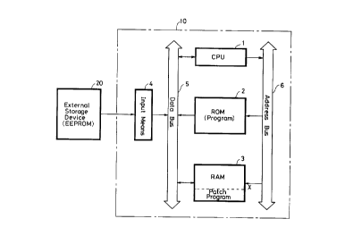
FIG. 1 is a block diagram showing a circuit
arrangement of an electronic device according to an
embodiment of the present invention;
FIG. 2 is a diagram used to explain the
electronic device according to the present invention;
FIG. 3 is a diagram used to explain the
electronic device according to the present invention;
and
FIG. 4 is a flowchart to cahich references will
be made in explaining operation of the electronic
device according to the present invention.
DETAILED DESCRIPTION OF THE PREFERRED EMBODIMENT
The present invention will hereinafter be
described with reference to the drawings.
In FIG. 1 of the accompanying drawings,
reference numeral 10 generally designates an overall
arrangement of a one-chip microcomputer serving as an
electronic device. The electronic device 10 includes
a CPU (central processing unit) 1 serving as a
processing means, a ROM (read only memory) 2 serving
as a fixed memory means, a RAM (random access memory)
3 serving as a variable memory means, an input means
4 or the like. The CPU 1, the ROM 2, the RAM 3 and
the input means 4 are connected to one another via a
data bus 5. An address output formed by the CPU 1 is
supplied through an address bus 6 to address inputs
of the ROM 2 and the RAM 3.
An external storage device 20 is connected to
the input means 4. This external storage device 20
also is disposed within the electronic device 10.
The external storage device 20 is formed of, for
PATENT
-5-
example, an EEPROM (electrically erasable and
programmable ROM) in which there are generally stored
parameters, etc., obtained in the adjustment process
of the electronic device. An information from the
external storage device 20 is supplied through the
input means 4 to the RAM 3, in which it is stored so
as to be utilized in the processing in the CPU 1.
In such electronic device 10, an information of
a processing program at the CPU 1 is stored in the
ROM 2 in a fixed state. In this processing program,
there is provided a command which executes a
processing in accordance.with an information stored
in a predetermined address X of the~RAM 3 at every
predetermined cycle. In the external storage device
20, there are stored an information (described later
on) for patching a bug of the information stored in
the ROM 2, if necessary, together with the above
parameters obtained in the adjustment process.
As shown in FIG. 2 of the accompanying drawings,
in the ROM 2, there is initially provided an
activation program. Then, there is provide a
processing program for the CPU 1. This processing
program includes a command for calling (CALL) the
predetermined address X of the RAM 3, for example, at
every predetermined cycle.
In the predetermined address X of the RAM 3,
there is stored an information for patching a bug of
the information stored in the ROM 2 from the external
storage device 20 through the input means 4. More
specifically, in FIG. 3 of the accompanying drawings,
when the information stored in the ROM 2 has no bug,
a return (RET) command is provided~in the
predetermined address X. On the other hand, when the
information stored in the ROM 2 has a bug, there is
provided a program for patching the bug of the
~~8~8~~
-6-
PATENT
information from the predetermined address X of the
RAM 3.
The return (RET) command is provided at the end
of the patch program.
Therefore, an operation shown in a flowchart of
FIG. 4, for example, is carried out in the electronic
device 10.
Referring to FIG. 4, when the power switches of
the electronic device or electronic apparatus 10 are
turned on, at step S1, an information from the
external storage device 20 is stored in the RAM 3.
It is determined in the next decision step S2 whether
or not the read information includes the program for
patching the bug on the information stored in the ROM
2. If a NO is output at decision step S2, then the
processing proceeds to step S3, whereat a return
(RET) command is written in the predetermined address
X of the RAM 3.
If the read-out information has the patch
program for patching the bug as represented by a YES
at decision step S2, then the processing proceeds to
step S4, whereat the bug patch program from the
external storage device 20 is written in the
predetermined address X of the RAM 3. The end of
this patch program includes a return (RET) command.
In the next step SS, the processing is executed
in accordance with the information program stored in
the ROM 2 by the CPU 1. In step S6, the predetermined
address X of the RAM 3 is called (CALL). Thus, in
step S7, the processing is executed in accordance
with the bug patch program from the predetermined
address X of the RAM 3 by the CPU 1. After step S7
was ended, the processing is returned to step S5.
As described above, according to the electronic
device of the present invention, although the defect
- - ~ ~ PATENT
of the information stored in the fixed memory means
(ROM 2) is once executed, the bug is patched by the
information from the variable memory means (RAM 3)
and the bug on the program can be compensated for
totally. Therefore, the design of the existing
electronic device 10 (CPU 1, ROM 2, RAM 3, input
means 4, etc.) itself need not be varied and the bug
that was discovered after the electronic devices had
been mass-produced can be patched.
In the above-mentioned flowchart, steps S1
through S6 are.all executed in accordance with the
program stored in the ROM 2. Further, in the above-
mentioned program, the call (CALL) command and the
return (RET) command can be executed by using jump
(JMP and JUMP return) commands.
As the bug in the information stored in the ROM
2 and which can be patched in the above-mentioned
apparatus, there can be expected erroneous display on
,the display unit or the like. That is, in the
erroneous display caused by the bug on the program,
such erroneous display is erased by the patch program
after the erroneous display was made. Alternatively,
if a correct display is made, then an instantaneous
erroneous display can be immediately patched although
the erroneous display occurs. Therefore, the users
cannot know such erroneous display.
It is expected that bugs on the information
stored in the ROM 2 and which can be patched by the
above-mentioned apparatus constitute about 30 to 40%
of all bugs. Accordingly, if the bugs cannot be
patched by the above-mentioned apparatus, electronic
devices, etc., must be mass-produced one more time.
However, patching of the bugs with the above ratio
can achieve remarkably large effects from a
manufacturing standpoint.
2~~6~~~
_g_
PATENT
According to the present invention, the bug on
the information stored in the fixed memory means is
patched by the information from the variable memory
means. Therefore, the bug that was discovered after
the electronic device had been mass- produced can
patched without changing the design of the existing
electronic device.
Having described a preferred embodiment of the
invention with reference to the accompanying
drawings, it is to be understood that the invention
is not limited to that precise embodiment and that
various changes and modifications thereof could be
effected by one skilled in the art without departing
from the spirit or scope of the invention as defined
in the appended claims:
m