Note : Les descriptions sont présentées dans la langue officielle dans laquelle elles ont été soumises.
2~89~43
OPTICAL MAGNETIC FIELD SENSOR
The present inventlon relates to an optlcal magnetlc
fleld sensor, partlcularly an optlcal magnetlc field sensor
whlch can measure a magnetlc fleld strength wlth hlgh
preclslon uslng Faraday's effect.
Heretofore, varlous structures of the optlcal
magnetlc fleld sensor have been known whlch uses Faraday's
effect for measurlng a magnetlc fleld strength. As an
example, JP-A-61-82,179 lald-open on Aprll 25, 1986 dlscloses
a method of measurlng a magnetlc fleld strength capable of
maklng the measurement wlth hlgh preclslon whereln a llght
beam lntenslty ratlo of two (P and S) polarlzed llght beams
passed through a Faraday element and emltted from an analyzer
ls used to correct errors resultlng from llght beam losses at
the llght beam transmlsslon paths whlch are not relatlve to
the Faraday's effect.
In the technlque of the above JP-A-61-82,179 lald-
open on Aprll 25, 1986, a llght beam lntenslty ratlo a
(=Jl/J2) of a P polarlzed llght beam lntensity Jl to a S
polarlzed llght beam lntenslty J2 emltted from an analyzer ls
prellmlnarlly determlned at the tlme when a magnetlc fleld ls
not applled on the optlcal magnetlc fleld sensor, and a
treatment of regularlzatlon of slgnals at the tlme of
recelvlng the slgnals when a magnetlc fleld ls applled on
- 64881-413
20899~
64881-413
the optical magnetic field sensor is performed wherein
the S polarized light beam intensity J2 is multiplied by
the above ratio a, so that the errors resulting from
light beam losses at the light transmission paths can be
0fi corrected. However, the technique of JP-A-61-82,179
performs merely the treatment of regularization of
signals of multiplying J2 by the above ratio a, so
that signal errors resulting from temperature could not
be corrected and a problem arose in that it can not be
used as a highly precise optical magnetic field sensor
suitable for use at large temperature change.
An object of the present invention is to obviate
the above problem so as to provide an optical magnetic
sensor which can measure a magnetic field strength with
16 high precision without measuremental errors resulting
from temperature change.
Other objects of the present invention will
become apparent from the ensuing descriptions and claims
and attached drawings.
Now, the above objects can be achieved by the
present invention.
The present invention is an optical magnetic
field sensor, comprising a light source, a polarizer
which changes a light beam emanated from the light source
through an optical fiber transmission path into a linear
polarized light beam, a Faraday's element which gives a
2s8q943
Faraday's effect to the linear polarized beam depending on an
applied magnetic field, an analyzer which separates the linear
polarized llght beam glven wlth the Faraday's effect into a S
polarized light beam and a P polarized light beam, a first
light beam-receiving element which receives and changes the S
polarized llght beam into an electrlc slgnal Vl dependlng on
the beam intenslty, a second llght beam-receiving element
whlch recelves and changes the P polarized light beam into an
electric signal V2 dependlng on the beam intenslty, a first
calculation circuit which is supplied wlth the electrlc signal
Vl having a dlrect current component DCl from the flrst light
beam-recelvlng element to obtain an output Vll based on an
equation Vll=(Vl-DCl)/DCl, a second calculatlon clrcuit which
is supplied wlth the electrlc signal V2 having a direct
current component DC2 from the second light beam-recelving
element to obtain an output V22 based on an equatlon V22=(V2-
DC2)/DC2, and a third calculation circuit which is supplied
with the outputs Vll and V22 (whlch are optlonally reversed
and multlplled) obtained from the first and second calculatlon
circults by outputs treatment of obtainlng an output V3 based
on an equation V3=l/(a/vll+~/v22) when Vll V22 P
values or an equation V3=1/(a/V~ /V22) when 11 22
negative values, wherein a and ~ are constants and a+~=l, the
output of V3 of
64881-413
20899~3
the third calculation circuit being a decisive value for
obtaining a magnetic field strength.
The optical magnetic field sensor of the present
invention has the structure as mentioned above of adding
06 the third calculation circuit to the structure of an
optical magnetic field sensor which is substantially the
same with conventional ones, so that measuremental errors
caused by losses in the light beam paths are excluded by
the treatment of regularization of the signals, and
measuremental errors caused by temperature change are
excluded from the signals from the first and second
calculation circuits by the calculation at the third
calculation circuit. Therefore, a magnetic field
strength can be measured with high precision.
lh For a better understanding of the present
invention, reference is made to the accompanying
drawings, in which:
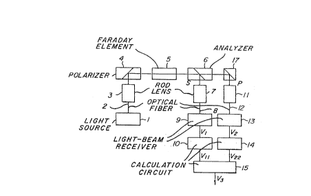
Fig. 1 is a schematic block diagram showing a
structure of an embodiment the optical magnetic field
sensor of the present invention;
Fig. 2 is a schematic block diagram showing a
structure of an optical magnetic field sensor of a
comparative example;
Figs. 3a, 3b and 3c is a characteristic graph an
embodiment of the present optical magnetic field sensor
showing an example of temperature characteristic
2DB~943
64881-413
property relative to V11 output change ratio, V22 output change
ratio, and V3 output change ratio, respectively.
Figures 4a, 4b and 4c is a characteristic graph of the
present optical magnetic field sensor showing another example of
temperature characteristic property relative to V11 output change
ratio, V22 output change ratio, and V3 output change ratio,
respectively; and
Figure 5 is a characteristic graph of the present
optical magnetic field sensor showing still another example of
temperature characteristic property relative to V3 output change
ratio.
Numbering in the Drawings
1 ... light source
2 ... optical fiber
3 ... rod lens
4 .... polarizer
5 ... Faraday's element
6 ... analyzer
7 ... first rod lens
8 ... first optical fiber
9 ... first light beam-receiving element
10 ... first calculation circuit
11 ... second rod lens
12 ... second optical fiber
13 ... second light beam-receiving element
14 ... second calculation circuit
15 ... third calculation circuit
20899~3
64881-413
Hereinafter, the present invention will be explained in
more detail with reference to examples.
Example 1
Referring to Figure 1 showing a structure of an
embodiment of the present optical magnetic field sensor, reference
numeral 1 is a light source made of LED, 2 is an optical fiber
forming a light beam transmission path, 3 is a rod lens which
causes distributed light beams to parallel light beams, 4 is a
polarizer which makes a light beam to a linear polarized light
beam, 5 is a Faraday's element made of Bi12SiO20 which causes the
linear polarized light beam to rotate to give Faraday's effect
depending on a given magnetic field strength, and 6 is an analyzer
which separates a given linear polarized light beam into a S
polarized light beam and a P polarized light beam.
In addition, reference numeral 7 is a first rod lens for
condensing parallel light beams of the analyzer 6, 8 is a first
optical fiber forming a light beam transmission path, 9 is a first
light beam-receiving element made of a photodiode for converting
the S polarized light beam into an electric signal depending on
the strength thereof, 10 is a first calculation circuit for
20899~3
calculating and multiplicating the converted electric
signal to exclude measuremental errors and the like
resulting from losses in the light beam path, 11 is a
second rod lens for condensing parallel light beams of
Ofi the P polarized light beams separated at the analyzer 6,
12 is a second optical fiber forming a light beam trans-
mission path, 13 is a second light beam receiving element
made of a photodiode for converting the P polarized
light beam into an electric signal depending on the
strength thereof, and 14 is a second calculation circuit
for calculating and multiplicating the converted electric
signal to exclude measuremental errors and the like
resulting from losses in the light beam path. The multi-
plication ratio in the first calculation circuit 10 is
1~ equal to that in the second calculation circuit 14.
The structure just described above is substan-
tially the same with the prior optical magnetic field
sensor, however a characteristic feature of the present
invention is the provision of a third calculation circuit
15 which is supplied with the outputs from the first and
second calculation circuits 10, 14 to perform a desired
calculation so as to exclude measuremental errors
resulting from temperature change. That is, the third
calculation circuit 15 is supplied with the output Vll
from the first calculation circuit 10 and the output V22
from the second calculation circuit 14, the outputs Vl1
208q943
and V22 belng optlonally reversed and multlpllcated, to
calculate and obtaln the output V3 based on the equatlon
V3 lt(a/Vll ~/V22) when Vll-V22 are positlve values or the
q on V3 1/(a/Vll-~/V22) when Vll-V22 are negatlve values,
whereln a and ~ are constants and a+~=l.
Herelnafter, modes of operatlon of the present
optlcal magnetlc fleld sensor of the aforementloned structure
at the respectlve calculatlon clrcult wlll be explalned.
When the wave length of the llght beam emanated from
the llght source 1 ls taken as 850 nm, the length ~ of an
element of a slngle crystal B112S102o ls taken as Q=4.02 mm,
and the lntenslty of the lncldent llght beam from the llght
source 1 ls taken as Iol the lntensltles Il, I2 ~f the output
llght beams at the flrst and second llght beam-recelvlng
elements 9, 13 are expressed by the followlng formula:
Il = Io/2{Q-2~00~TQ-2~Ve+~Ve~T)HQ} ~ ~ ~ ~ . (1)
I2 = Io/2{Q+2~00~TQ+2(Ve+~Ve~T)HQ} . . . . . (2)
whereln
~00: Temperature change ratlo of natural llght rotatlonal
ablllty
~T: Temperature variation from 25~C
Q: Length of the slngle crystal element
Ve: Verdet's constant
~Ve: Verdet's constant temperature change ratio
64881-413
2089943
H : Alternate current magnetic field strength
In the first and second calculation circuits 10,
14, the circuits are supplied with the electric signals
Vl, V2 from the first and second light beam-receiving
o~ elements 9, 13, respectively, the electric signal Vl and
V2 having respective direct current components DCl and
DC2, to obtain the outputs Vll and V22 of the following
formula based on the equations of Vll=(Vl-DCl)/DCl and
V22=(V2-DC2)/DC2.
Vll = -2(Ve+~VeAT)He/(1-2A~o~T~) ....... (3)
V22 = 2(ve+~veAT)H~ +2~o~T~) .......... (4
In this case, if V3 is defined as
V3=l/(~/Vll-~/V22) and a+~=l, the following formula (5)
can be obtained.
1~ V3 = -2(Ve+AVeAT)He{l-2(2~-1) A~oATe} ....... ( 5)
Therefore, in order that the output V3 expressed
by the formula (5) is not dependent on temperature, it
is only necessary to fulfill the following formula (6).
V3(AT) = V3(AT=0) ....... (6)
Accordingly, a value a of ~=(l-~Ve/2VeA~oATe)/2 is
obtained to derive values of ~=0.6805 and ~=0.3195 in
this embodiment.
Considering that Vll and V22 are obtained as
positive values in practice, the output V3 of the third
calculation circuit 15 is newly defined as:
V3=l/t~/Vll+~/V22)~ wherein ~+~=1.
- 10-
2089943
Example 2
Three types of optlcal magnetlc fleld sensor
conslstlng of an embodlment of the present lnventlon of the
above structure, the comparatlve example of the structure, as
shown ln Flg. 2 and a prlor example of JP-A-61-82179 lald-open
on Aprll 25, 1986 as explalned above were actually prepared to
obtaln a relatlon between the magnetlc fleld strength and the
output, output change due to change of the amount of the llght
beam, and output change due to temperature change,
respectlvely. As a result, the followlng data as shown ln the
followlng Table 1 were obtalned to ascertaln that the output
V3 can be measured ln proportlon wlth the alternate current
magnetlc fleld strength H ln the embodlment of the present
lnventlon wlthout dependlng on output changes due to change of
the amount of the llght beam or loss ln the llght transmlsslon
path and change of temperature as compared wlth the
comparatlve example and the prlor example.
Moreover, ln the embodlment of the present
lnventlon, the temperature of the sensor was varled ln a range
of -20~C through 80~C, and output change ratlos relatlve to
the output at 25~C were measured to evaluate the temperature
characterlstlc property of the present sensor. The results
are shown ln Flgs. 3a-3c. As seen from Flgs. 3a-3c, lt can be
understood that the output V3 of the thlrd calculatlon clrcult
15 whlch ls a
64881-413
2089943
characteristic feature of the present invention was not
at all influenced by temperature change, even when the
outputs Vll and V22 of the first and second calculation
circuits 9, 13 were influenced by the temperature
change.
Table 1
\ Item Relation between Output change Output change
\ magnetic field due to change due to
\ strength and of light beam temperature
Example \ output amount change
Comparative Proportional None Yes
Prior Proportional None Yes
Invention Proportional None None
Though the temperature characteristic property
in the above embodiment is not always o% at the values
of the constants ~=0.6805 and ~=0.3195 due to errors in
the element length and errors resulting from increase-
ment of the effective element length caused by oblique
bonding of the elements, however, even in such a case,
the temperature characteristic property can be made 0%,
if the constants ~, ~ are deductively derived from
actually measured temperature characteristic properties
of Vll and V22 and the thus obtained optimum ~, ~ are
used to the outputs treatment or regularization of the
signals at the third calculation circuit 15.
For instance, in case when the element length e
-12-
2089943
is short resulting from an error or the like and the
temperature characteristic properties of Vll and V22 are
as shown in Figs. 4a and 4b, the temperature character-
istic property of the output V3 changes as shown in
Oh Fig. 4c, if the above values are treated in the third
calculation circuit 15 using the values of ~=0.6805 and
~=0.3195. Then, from the outputs Vll and V22 at -20~C
and the outputs Vll and V22 at 80~C, the constants ~,
are deductively derived as follows, namely from the
formula (7).
~/Vll(-20~C)+~/V22(-20~C)=~/Vll(80~C)+~/V22(8~~C) .. (7)
As a result, in the embodiment wherein the
element length is shorter than normal one, values of
~=0.7222 and ~=0.2778 were obtained which gave the tem-
1~ perature characteristic property V3 as shown in Fig. 5by the outputs treatment, showing clearly that the
outputs can be treated in the third calculation circuit
15 by using the deductively derived values of
As clearly apparent from the foregoing
explanations, according to the present invention, the
present optical magnetic field sensor can achieve
measurements of a magnetic field strength with high
precision, because it has further the third calculation
circuit in addition to the structure of the optical
magnetic field sensor having substantially the same
structure as that of conventional one thereby to exclude
-13-
2089943
measuremental errors caused by temperature change from
the outputs obtained from the first and second calcula-
tion circuits by virtue of the determined the outputs
treatment at the third calculation circuit. Moreover,
0~ measuremental errors caused by change of the amount of
the light beam emanated from the light source and losses
in the light beam transmission paths can be excluded
because it performs calculations for regularization of
the outputs at the first and second calculation circuits
in the same fashion as in conventional ones.
Although the present invention has been
explained with specific examples and numeral values, it
is of course apparent to those skilled in the art that
various changes and modifications are possible without
1~ departing from the broad spirit and aspect of the
present invention as defined in the appended claims.
ao
2~
-14-