Note : Les descriptions sont présentées dans la langue officielle dans laquelle elles ont été soumises.
20902~6
TECHNIQUE FOR CANCELLING SIGNAL DISPERSION
IN COMMUNICATIONS SY~ I ~;~S
Technical Field
The present invention relates to a signal dispersion cancellation
S technique and, more particularly, to a technique which is suitable for cancelling
ghosts in a television channel.
Back~round of the Invention
Signal dispersion, such as echoes, ghosts, multipath and intersymbol
interference, is an ever-present reality in co.~ c~tions systems. The severity of
10 this problem varies with the system application and, at times, can render a system
completely inoperative. For example, signal ghosts or echoes at levels which aremerely objectional to the viewer of a conventional television signal can render a
high-definition television (HDTV) signal unintelligible. Accordingly, cancellation
or compensation for such dispersion cannot be ignored.
Ghosts in a television channel can be categorized as being either
precursor or postcursor. A precursor ghost is one that precedes its associated
tr~n~mitte~ signal while a postcursor ghost is one that succeeds its associated
tr~n~mitted signal. FIG. 1 shows a typical ghost canceller structure 100 which
includes a feedforward finite impulse response (FIR) filter 101 and an infinite
20 impulse response (IIR) filter 102 in c~c~ . IIR filter 102 includes a feedback FIR
filter 103 and combiner 104, the latter subtracting the output of feedback FIR
filter 103 from the output of feedforward FIR filter 101. The feedforward FIR filter
equali~s the main signal and any precursor ghosts while the IIR filter, also known as
the feedback section, coll,pensates for the one of more postcursor ghosts. The
25 dispersion of the signal defines the required length or span of the feedback FIR filter
and is the most difficult part of the ghost canceller structure to implement. While the
exact position of any ghosts relative to an associated signal can vary from one
application to the next, ghosts in a television channel are generally widely separated
from one another and extend over a large time span. For example, the time interval
30 between the furthest precursor and po~cul~or ghosts associated with the same
transmitted signal can be 40~ seconds.
One prior art technique for implementing the feedback FIR filter in IIR
filter 102, refened to as the full-span approach, is shown in FIG. 2. This approach
involves implementing the feedback FIR filter using a data memory 201 and tap-
35 weight coefficient store 202. In typical ghost cancellation applications, data
2 4 ~
-- 2 --
memory 201 must have the capacity to store several hundred signal samples, and
tap-weight coefficient store 202 must provide one tap-weight coefficient for each stored
signal sample. At the incoming signal sample rate, each of the stored signal samples in
data memory 201 must be multiplied by its associated tap-weight coefficient in data store
202 via multiplier 203 and the sum of these products coupled to combiner 104. While
the full-span structure provides satisfactory ghost cancellation, it is very costly to
implement since the incoming signal sample rate is high, e.g., 14.3 MHz, and many
high-speed multiplications must be performed at this rate. In addition, the structure is
inefficient since most of the tap-weight coefficients have a value of zero due to the wide
time separation between ghosts.
FIG. 3 shows another prior art approach, referred to as the segmented-sparse
technique, to implement the feedback FIR filter in IIR filter 102. This technique
involves the use of variable delay random access memory segments 301-1 through 301-N
which are inserted between a plurality of FIR filters 302-1 through 302-N. The outputs
of such filters are combined by multiplier 303. While this approach reduces the
hardware required compared to the full-span approach, its rigid architectural structure
still requires circuit overdesign to meet the required performance goals. For example, if
the delay between adjacent ghosts is greater than the maximum delay provided by one
memory segment, two or more such memory segments must be concatenated and use ofthe FIR filter
disposed between such segments is lost. Alternatively, when the ghosts are
closely-spaced, more than one FIR filter is required between adjacent memory segments
and use of a number of memory segments will be lost. As a result, depending on the
locations of the ghosts, there is often an underutilization of either FIR filters or memory
segments with the segmented-sparse technique.
Accordingly, it would be extremely desirable if a more flexible ghost
cancellation structure could be provided which fulfilled both the necessary performance
and cost objectives.
Summary of the Invention
In accordance with the present invention, the limitations of prior art signal
dispersion cancellation arrangements are overcome through the use of a structure which
receives signal samples having an incoming sample rate, stores these signal samples in a
first memory and then writes these samples into at least one second memory. Writing of
-- 3 --
the samples into each second memory is performed at a submultiple of the incoming
sample rate. The samples stored in each second memory are then coupled at the
incoming sample rate to an FIR filter associated with each second memory. In thedisclosed embodiments which pertain to the cancellation of ghosts associated with
S television signals, a plurality of second memories is utilized and apparatus is provided
which enables any sample in a second memory to be provided to the associated FIR,
filtered therein and outputted at a time related to the position of any ghost.
In accordance with one aspect of the present invention there is provided an
apparatus for elimin~ting signal dispersion in incoming signal samples having a sample
rate, said apparatus comprising: first means for storing said incoming signal samples at
said sample rate; at least one second means for storing signals, each second storing
means being connected to said first storing means; at least one filter means for removing
signal dispersion; and means for providing signal samples from said first storing means
to each of said second storing means at a submultiple of said sample rate and for then
providing said signal samples in said second storing means to said filter means at said
sample rate.
In accordance with another aspect of the present invention there is provided a
method of elimin~ting signal dispersion in incoming signal samples having an incoming
sample rate, said method comprising the steps of: storing said incoming signal samples in
a first storing device at said incoming sample rate; providing the stored signal samples in
said first storing device to at least one second storing device at a submultiple of said
incoming sample rate; and providing the stored signal samples in each second storing
device to an associated filter at said incoming sample rate.
Brief Description of the Drawin~.~
FIG. 1 is a block-schematic diagram of a prior art ghost canceller;
FIG. 2 is a block-schematic diagram of a first prior art approach for re~li7ing
the feedback FIR filter shown in FIG. l;
FIG. 3 is a block-schematic diagram of a second prior art approach for re~li7ingthe feedback FIR filter shown in FIG. I;
FIG. 4 is a block-schematic diagram of a first embodiment of the present
invention for providing the feedback FIR filter shown in FIG. 1;
FIG. 5 is a block-schematic diagram of a second embodiment of the present
invention for providing the feedback FIR filter shown in FIG. I; and
~,
"~: ~
'= -
- 3a-
FIG. 6 is a block-schematic diagram of third and fourth embodiments of the
present invention for providing the feedback FIR filter shown in FIG. 1.
Detailed Description
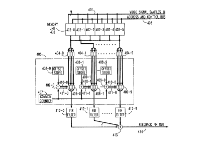
FIG. 4 shows an illustrative embodiment of the present invention for re~li7ing
feedback FIR filter 103 of FIG. I in a manner which compensates for 10 widely
separated ghosts in a television channel. In this embodiment, incoming 9-bit video signal
samples are supplied on bus 401 to memory 402 and written in consecutive locations
therein under the control of write signals on bus 403. To conserve power, memory 402
is advantageously a random access memory (RAM) having six sections designated as402-0 through 402-5. Each section has the capacity to store 128 9-bit samples, and the
total capacity of memory 402 is at least equal to the expected time span between a
received video signal and the last postcursor ghost associated with that received video
slgnal.
In the illustrative embodiment of FIG. 4, the total capacity of memory 402 is 768 signal
samples.
The incoming signal sample rate is 14.32 MHz. To reduce the required clock
speed, a plurality of signal samples is read out of memory 402 into one of second
memory units 404-0 through 404-9 on each read signal coupled on bus 403. More
specifically, for this application, four contiguous signal samples from memory 402 are
written into one of second memory units 404-0 and 404-9 on each read signal on bus
403. In effect, then, each section of memory 402 from the standpoint of the readoperation is viewed as storing thirty-two 36-bit "quadruple
20so~
samples". The write and read signals are arranged on bus 403 so each write signal is
followed by three read signals in each incoming signal sample period,
i.e., 14 321MH . Therefore, between five consecutive write signals there are twelve
read signals. Ten of these twelve read signals are used to control the reading out of
5 signal samples from l~ell-ol~ 402 into a different one of memory units 404-0 through
404-9. The rem~ining two out of the twelve read signals are not used. It should be
noted that the ten read operations are fully independent. Each read operation
accesses a different set of four consecutively stored samples from any of the sections
of memory 402 and couples these samples to any one of memory units 404-0
10 through 404-9. The above-described structure has many advantages. For example,
this structure can advantageously be arranged via software to direct any set of four
consecutively stored samples to any FIR filter. As a result, multiple FIR filters can
be supplied with the ap~ .iate samples so as to function as a single con~aten~ted
FIR filter. In addition, since the FIR filters need not have the same number of tap-
15 weight coefficients, one or more such filters could have more tap-weight coefficients-
and be supplied with those samples necess~ry for cancelling more severe ghosts.
While a plurality of signal samples is read out of memory 402, it should
be appreciated that due to the structure of a RAM, only certain sets of four samples
can be read out. That is, to retrieve multiple samples with each read, memory 402 is
20 viewed as storing 192 36-bit quadruple samples and each of these 192 quadruple
samples can be retrieved and fed to memory units 404-0 through 404-9. With such
multiple retrieval, each of memory units 404-0 through 404-9 must be replenishedwith new samples at a subm-lltirle of the incoming video sample rate if each such
memory unit is to provide samples to its associated FIR filter at the incoming video
25 rate. In the disclosed embodiment, the incoming video sample rate is 14.32 MHz
and the submultiple of the incoming video sample rate is 1 ~ 324MHz . However,
due to the location of the ghosts in the time domain in a particular application, it may
be necessary that the secondt third or fourth one of the retrieved quadruple samples
coupled to one of the memory units 404-0 t~Lrough 404-9 is processed by its
30 associated FIR filter at the same time that the first of the four samples in another one
of such memory units is processed by its associated FIR filter. To provide this
capability, the present invention advantageously utilizes a "fine-addressing" scheme
in connection with each of the memory units 404-0 through 404-9.
- 5 -
As mentioned, the resolution of ghost locations using the addressing of the
memory 402 is limited to an increment of n, where n is four in the illustrative
embodiments. Therefore, alignment of ghost locations within memory 402 is limited to
S L/n positions, where L is the span of memory 402, i.e., 768 signal samples. To provide
cancellation of ghosts with a finer resolution, the embodiment of FIG. 4 utilizes fine
addressing apparatus 405. Apparatus 405 includes a plurality of memories 406-0 through
406-9 wherein each such memory is associated with a different one of memories 404-0
through 404-9 and is the same size as its associated memory. Apparatus 405 also includes
a common counter 407, offset stores 408-0 through 408-9 and modulo n adders 409-0
through 409-9 wherein the offset stores and adders are respectively associated with
memories 406-0 through 406-9. It should be appreciated that the determination of the
offset counts provided by offset stores 408-0 through 408-9 are determined usingwell-known techniques and are a function of the ghost spacing.
Common modulo n counter 407 counts by ones from 0 to n-1 and then resets or
"wraps" around to 0. The counter output is supplied as an input to each modulo n adder.
The other input to each adder is provided by a different associated one of offset stores
408-0 through 408-9. Each modulo n adder sums the current count of common counter
407 with the offset count provided by the associated offset store and resets or overflows
upon reaching the sum n. Upon overflow, adders 409-0 through 409-9 respectively
generate a signal on leads 410-0 through 410-9. The overflow signal provided by each
adder serves as a signal to respectively write the samples from a different one of memories
404-0 through 404-9 to the associated one of memories 406-0 through 406-9. The sum
provided by each modulo n adder on leads 411-0 through 411-9 is coupled to the
associated one of memories 406-0 through 406-9 and serves as a read pointer for that
memory. Accordingly, by storing the appropriate offset value for each of memories 406-0
through 406-9, any of the four samples in one of these memories can be simultaneously
read out with any of the four samples stored in a different one of these memories.
Each of FIR filters 412-0 through 412-9 is associated with a different one of
memories 406-0 through 406-9. Each sample read out of the memories 406-0 through406-9 is coupled to its associated FIR filter. Each FIR filter includes a tapped delay
line into which the received signal samples are successively stored and forwarded
therethrough. The received signal sample stored in each separate storage location or
"tap" is respectively multiplied by an associated tap-weight coefficient and theproducts thus formed are summed. The tap-weight coefficients each have a
~'
~ 2090~
value which is a function of the ghost characteristics and which may be deterrnined
using well-known techniques. Summer 413 combines the outputs from each of the
FIR filters 412-0 through 412-9 to provide the feel1b~ck FIR filter output on
lead 414.
Alternative structures which provide the fine addressing capability of
apparatus 405 are also possible. Such alternative structures are shown in FIGS. S
and 6. In FIG.S, the operation of memories 402 and 404-0 through 404-9 are
identic~l to that described with respect to FIG.4. To provide fine addressing
capability, a number of FIR elements are added to each of FIR filters 412-0 through
10 412-9. In general, the number of such FIR elements added to each FIR filter is equal
to n-l. In the disclosed embodilllents, n = 4 and the additional FIR elements are
designated in FIG.S as 501, 502 and 503. Each of these additional FIR elements as
with each of FIR elements of the tapped delay line following element 503 provides a
data delay of the reciprocal of the incoming video sample rate and has an associated
15 tap-weight coefficient. We may view these tap-weight coefficients of the expanded
tapped delay line, i.e., including elements 501-503, as forming an ordered sequence
with the tap-weight coefficient associated with FIR element 501 as the first
coefficient in such sequence. Now, depending on the offset count required in FIG.4
based on ghost spacing, certain of the tap-weight coefficients in the ordered sequence
20 will be zero. For example, to provide the equivalent effect of a stored offset count of
3 in FIG. 4, the first tap-weight coefficient associated with FIR element 501 will be
non-zero as will be that associated FIR element 502, etc., until the last three tap-
weight coefficients in the ordered sequence which will be zero. Similarly, to provide
the equivalent effect of a stored offset count of 2, 1 and 0 in FIG. 4, then the first
25 non-zero tap-weight coefficiçnt is ~ ~c~ ely associated with FIR elements 502,
503 and the first FIR element in the tapped delay line following element 503.
FIG. 6 shows third and fourth possible arrangements for providing the
fine addressing capability of FIG. 4. In FIG. 6, the operation of memories 402,
404-0 through 404-9 and FIR filters 412-0 through 412-9 operate as in FIG. 4. To30 provide the n-l desired offset, a pro~~ able delay element 601-0 through 601-9 is
respectively disposed between FIR filters 412-0 through 412-9 and summer 413.
Each programmable element can provide a delay of between zero and n-l signal
sample periods wherein the amount of such delay is equal to the n-l minus the
desired offset. Alternatively, the position of programrnable delay elements 601-0
35 through 601-9 could also be respectively disposed before FIR filters 412-0 through
2~9~2~'~
- 7 -
412-9. These alternative positions of the delay elements are shown by dotted lines in
FIG. 6.
It should, of course, be understood that while the present invention has
been described in reference to the disclosed embodiments, other arrangements mayS be app~ellt to those of ordinary skill in the art without departing from the spirit and
scope of the present invention. For example, while in the disclosed embodiments,memory 402 is a single port RAM which utilizes shared access of read and write
signals via bus 403, a dual-port RAM could be used so that the read and write signals
could be independent of one another and, as a result, the number of FIR filters could
10 be increased from the maximum of 12 in the disclosed embodiments. Furthermore,
while in the disclosed embodiments, the writing of signal samples into memory 402
is done at the incoming signal sample rate, an additional buffer could be disposed in
front of memory 402 so that the writing operation for memory 402 could be done at
a submultiple of the incoming signal sample rate. This would also allow an increase
15 in the number of FIR filters. Moreover, while in the disclosed embodiments, each of
the FIR filters has been described as incorporating a tapped delay line, multipliers
and a summer, the function of such filters can be provided by one or more
ap~rol,liately pro~ ed general-purpose processors, or special-purpose integratedcircuits, or digital signal processors, or an analog or hybrid counterpart of any of
20 these devices. Finally, while the disclosed application of the present invention has
been described in reference to the cancellation of ghosts in television transmi~ion
appliration~, the present invention is not limited to such applications and, indeed,
may be utilized for the cancellation of signal dispersion in a wide variety of
co-~-.----ni~tions systems.