Note : Les descriptions sont présentées dans la langue officielle dans laquelle elles ont été soumises.
WO 93/05634 PCr/US92/07118
-1- 2091g99
SURFACE MOUNT ASSEMBLY OF DEVICES USING
AdCon INTERCONNECI IONS
Field of the Invention
This i~ ti~n is c~nr~ ed with ~ylJ~aluS for and pmcess of surface mount
5 ~sc~ ,ly of devices using AdCon ~ o~ ecl;
Back~!round of the ~vention
Flectrir~lly c~n~lVCI;~C adhesives are widely used in the elc~llu,~ics ih~du~
Llyollant app!;c~;ol-s include die-attach and ~ n~bly of printed wiring boards
(PWBs). An example of a device, 2, with a quad A- ~ of leads, 3, surface
10 .~un~ on a PWB, 4, to a co,l~n~l;ng plu~lity of cond~ t~. pads, 5, which, in
turn, are con.-ec~l to cond.,c~u~ s, 6, on the PWB folming a part of a larger
~ss~ h~ly, 1, is shown schc~ ;r~lly in FIG. 1. As device ~l;n.~ n~iQn~ CQI~l;nvC to
shrink, the r.. k.,.~ of leads on devices to be cQn~c~ to the PWBs cQnl;~ c to
il,.,l~ase and the ~3icl .nre k,t~. xn centers of adjacent leads or pads (known as a
15 "pitch") co ';---lcs to dc~ ase, it beco...Ps more Aiffirlllt to acc~ly place
isotropically cQn/ll~c~ adhesives wilhùut shorting adjacent leads. An alt~ ."ati~e
approach is to use anisotropically cQl~d-lc~ adhesives which cQI~ lcl only in the
~lu~;lion p~n~ to the board (z-direcdon).
Anisollu~iczlly con~ cl;~c adhesives, h~"Jn rt"~ called AdCons (for
20 Adhesive G~n~ t~ is a class of ebctnr~lly cQnd~cli~c adhesive m~ lc
fnrm~ tcA on the "bnd~ng" con~ The m~t~ ls are l~l~&~d by dispersing
c~ n ;c~lly co~d.,c1;~c p&~cles in an inc~ ring polymer matrLlc forming an adhesive
cc~ tc Typically, the adhesive c~.ni~C;~, is ~pplied to the surface of a PWB by
stenc~ , screen-printing or 1A.~;n~;ng a film of the c(~nAuctive adhesive A25 s~ hc ~ lc~Jlc~n~ n of a portion of pwB~ 4~ with cQn~llc tnr pads s~ a region of
AdCon, 7, on the PWB and a device 2 with leads 3 to be cQ.-n~eA to the co~ clor
pads, is shown in FIG. 2. After the device is placed onto thc PWB and a pl~rçment
f~e displaces the AdCon from ~t . ~n the cQI~ c t~n pads on the PWB substrate
and the leads on the device, a layer of AdCon with a !~;r~ ss of a singlc particle
30 ~,~u,s bct~.~n each lcad and cqn~ ct~ pad, as is shown srk~ ly in FIG. 3
Indi~idual ~ iclcs span the gap ~t-. ~n the devicc and PWB and form an electrical
int~ n~ n Similarly, se-~ Qn~1uctor chips with cond~ /e pads may be
surfacc .~ ~ on the PWB.
In the past, the fn~ iQn of AdCûn inb.,..on~ec1;0ns was typically
35 c~?r.du~ ~3 via serial plOCCSSCS wherc each p~c~e was ~li~ed~ placcd under
plCSS~ , and cured individually in a curing oven. ~ s of such pl~CCSS ng may
~L
Wo 93/05634 pcr/us92/o71 l8
2091999 -2-
be seen from U.S. Patent 4,667,401 issued on May 26, 1987 and U.S. Patent
4,868,637 issued on Septcmber 19, 1989, both to J~nes R. C'le~ et al. or fio
an article by Brian Sun "'The Paste r~ n~ ~ ' - Vertically Co~J~ Adhcs;~
r~.nnr,cl;QI- T~ , August 1988, pp. 31-32. However, this type of ~ s-:~ gS leads to an inadequate control of applied l,..,s;,u.~, which could vary from i.i--.rr~ nt
with f~"",~ n of non-co~tu~ g joints to cAces~ , with ~es~llts~t ~g ml~ of lcadsand int~..;Qn--r~ -c.~ These p~ccsscs werc ~iffir~ to implement both for high
inputJoutput (V~) surface-mount psrl~a~s and for very small chips, not only
G of their low lLU~lgl'l'U~, but also be~ ;e the A~5c~ l~SS~CS require
10 coplanarity of the PWB, the package, and an s-cs~mbly implement. Non-Flsnsrity in
t~he system can lead to problems with yield and reli~hility pc r.... ~sn~e r:~ll.-" ...o.~"
very small s~mico--duc~r chips need an ~rplir~tiQn of high forces per small areas,
wilLoul the danger of ~qm~ging the chips. Th~.~fo.e, there is a need for an err~ nt
~ne, for o.~, -;o-lling the above-noted lJlubk-.--c., incl~ ng a need for a IIl~CSS of
15 applying a ~ ;~Ul~ ul~irulll~ly across a device or devices of differing ll;...nn~ionc and
heightc, as well as for an al)p~ s for ;~q~k ~r~l;ng the process.
Summary of the Invcntion
Tt i~C in~ lioll is a~ .p--~nJ~ for and a process of batch ~csembly of
sundry leaded or padded devices, en~ t~ and non c ~ t~ onto a printed
20 wiring board (PWB), which eyhibitc signifir~nt i ~ lu~e~n~ in both
r~ hility and reli~hility. A plcs~ul~, frame ~csen~kl~ ~pp- nt~C p~_.llfi~ an
a~ n of ,--.:r ,....ly ~ictribvt~ ~ u~S to a variety of leaded F~c~s and
padded se ~.;r~ cl~ chips during cure of c~Juc~ , adhesives (AdCons), and
leads to the l~ ;nn of ~ nc in ini~al int~"CQnn~l;o~ lc,;~nce, and thereby
25 to the c~h~n~C"~ l of the reli~ility of AdCon inD~"~;Qnnr~!;on~ The pl~S~ul~S ale
-qrFli~ to the devices by an e~t~nql appli~a~ n of a fluid under pl~ Ul~ to a
fl~ c reQ~lirntly ~h~ 91~1e ~l~culbrdAc which co~ro~ hly envclops O~JI1;o~ s of
the devices and adjacent areas of the PWB. The e~te~nql applical;Q~- of pl~i~au~,
enh ~res thelTnql co~ needed for curing the AdCon, illcleases the range of30 ~ ss:ne pa~ usable for this ~ch~ uc and l~.luccs ~sc-~.bly times.
se-.~ yields of 100% were obsc,~d for a variety of surface ...-)....tud p~qCL'qgeS
g that the system will be highly reliable.
Wo 93/05634 pcr/us92/o7118
- 3 -
2091999
Brief De~iption of the Dra~in~
FIG. 1 is a schr ~ ;r ~.~ elJlc~-r ~O~ of a po~tion of a PWB
and of a quad device su~face-.~ t~d on the PWB;
FIG. 2 is a s~k~ ;r ..,~" s~ ;oA of a section of a PWB with a thin
S layer of AdCon thereon and a leaded c~ re c~ t pnor to the ~se .hly;
~ IG. 3 is a schc ~ ;r ~ s,~ n of the ~ ,...r.~t shown in FIG. 2
but with CQ~3~1C!;~_ C~ r~ (pads) on thc PWB in ~ ;Cal contact with leads of
the device via co.. hn;l;~re ~ icl~s of the AdCon aftcr an applir~ ion of y..,s~FIG. 4 is a frontal sC~ l;c eYrl~d~ view of a cross-section of the
0 pl~5~ , frame a~pdl~ltus used for the batch ~sembly of AdCon in~.cQI-~-
FIG. 5 is a frontal schc .~-l;r view of a cross sc~n of the p.~s~
frame a~p~ C of FIG. 4 but shown in a closed, opc ~ g ~ u~;
FIG. 6 is a s~:h~ -;r, ~ , eYpl~r~l view of the A~ s shown
in FIG. 4;
FIG. 7 is a s,rk~ l;r ~.~ view of the appa~atus shown in FIG. 5;
FIG 8 is a seh~ tir ~-~p~li~C ~plCSC ~ l;on of a po~tion of a PWB
with a quad device surface l.-O! ~ .t~ on the PWB and a cable pigtail COn~r~! ;on tO
the device.
FIG. 9 is a s~h~ ;c ~.~pCCli~C view of the ~l'P~ c shown in FIG. 6
20 inrly-1;ng a cable pigtail cQI.nc~ n.
Detailed Description
The ~csemhly of elc~,~unic circuits with ckc~;c~11y anisotropic
CQ~ adhc~ cs (~' d~'onc) versus the solder t ~ ~'ogy offers nu~ vus
ad~g~s for the mar ur~ of PWBs as well as for the effect on the
25 cn~i u ~, ~ Low ~ s .c~u led to cure the adhesives minimi7~ d~m~ç,
both tll~m~l and yh~icaL to packages and PWBs. Adhcsi~ st~s permit the
of fine pitch cQ~ c-fi~ oul the f~n~tinn of solder shorts or
in~m~ent~ and lead to a .~luc~ cost ~c5e ..bly ~ioce s~;n~ Enn,~,n.... ~ y,
arlisOl~ul~iCally CQn lu~ c adhcsi-cs c1;~..;n~ the need for c1e~nin~ flux residues
30 with cn~ n n~ lly harmful ch, ..-r~l~, such as chlw~Iluû.u~all,ons (CFCs), and
reduce workcr c l~ ~ ~s to lead ~om molten wave solder baths or rcflow ovens.
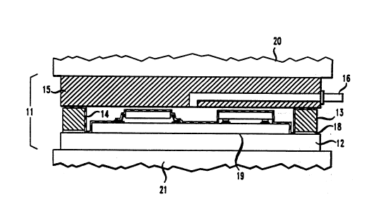
The a~p~alus forl, ,.cl;~-;n~ thc in~".Lion is sC~ I;c~lly ~ ,scn~d
in FIGs. 4 and 5. C~ s~onrlin~ ,c views of the a~p~lus are also shown
in FIGs. 6 and 7, ~s~ ,ly. For re~cnn~ of clarity the clr- 4 ls of the a~&~lus35 and thc dcvices arc not drawn to scale. The ~l)P~ S, shown in an cxploded vicw in
Wo 93~634 Pcr/uss2/o7l 18
2091999 -4-
FI&. 4 and grn~gl1y denoted by mm~.Q~ s a base, 12, a spacer, 13, a
G, 14, and a lid, 15, provided with an inlet, 16, for ihlh~l-~c;~g a s~its~le
fluid, such as air, under p.Y,S~., on top of cover 14. ~Ic....b.i..~c 14 is of fl~ibk
resiliently ~h~ hablc n~st~nQl such as polysiloysne rubber, sc~ d at the p~,- ;phc-
5 between the spacer and the lid. When subjcc~ to ~ , by in~ of fluidinto the l~ olu~ lcd by the lu~,~llbl~C and the lid, the ~l ~c
CO~ ;O~1Y co~ro-...~ to thc o~ rs of the surf. ces of devices, leads and adjacent
surf~oes of the PWB on the base 12. Care should be taken that the ~1_~bl~c~ prior
to the a~ liral;o~ of the ~ , evcnly spans the space above the devices,
10 prcferably in a taut ~nncl, will~oul kinks and wrinkles which could affect the
c~ f ~ r of the cover with the PWB and dcvices. Spacer 13 is providcd with at
least onc e~h~ port lB, pc.,l,il~ing e~p~ ion of air from bt"-r Ih cover 14. Spaccr
13 is ~o.idcd as a l~,.,o.able unit, primQrily for the pu.~oscs of f~Q~ilitQting cl~Qning
of floor, 19, of base 12. However, spacer 13 m. y be s~ulcd to basc 12 cither
15 pc~ rI.Ily or l~ . A grid (not shown) may bc provided, optionally, on or in
the floor, 19 of base 12. Thc grid could be in the form of a screen or an array of rods
on the floor or a grating formed in or on the floor of the base, and others. The main
pUllJO~ of the grid is to rcduce the pos~ihility of ~ ,~nce of air ~ocLet~ ~.~n the
bottom of the PWB and the floor of the base, and to fQ-cilitQ-te l~mo~,dl of the PWBs
20 from the basc after the a~ l;nll of plC,S~ul~ and heat
Inh~l-~ " of the fluid under yI~,s~ , leads to a ~ ndc nc~ for
co--q~nc~t pw of ~p~aluS, 11, e.g. base 12 and lid 15, to SC~ t~, each from
anolhcr. Th~ f~l~, the a~..lus should be providcd with some means to Lecp the
p~s ~g. lh~r. The app&alus may be held logctl,cr by means of clamps or bolts or
25 some other sec~ing means. ~Io~ ,., thesc may bc Culll~.~lllC to use and
assemble, and may present a danger of failurc. A viable al~."ah~c could be the use
of a simple press, such as a bookbindcr's prcss, operable in a suit~ble ulalulcr, e.g. by
means of a vertical screw or a leva. A m~re viable ~ would be the use of
an i~d~ type of a press, such as a lz-..;n~;ng press.
In the pl~,fe.,~d c-.. ho l;.. ~cnt, a~&~us 11 is positinn~ble bcl~.~n an~
upper and a lower platens 20 and 21, l~ cly, of a typical ~ DI;"~ press (not
shown). The ~l-,S~ul~ eYhihited by the press by the press ll~s~,~, ~ly of the
aypa~dtus should be surr~ rnl to keep parts of the al)pd~alus ~o~ , and to ~ ;cnt
le~1~a~ of the fluid bct-.~,c.l thc ,. ~b-; nc and the lid, but not so great as tD l~rna~e
35 ~lliOnS of u~m~ c 14 located ~I~.~n adjacent pollions of the spacer and the lid.
Base 12, spacer 13 and the fle~ible uIclllb~anc 14 are l~ O~ablc from the press for
Wo g3/05634 Pcr/US92/071 18
.
-s- 2091999
the pu~poses of placing on thc base articles to be ~ cc s~3 and ~, uo~mg the
s ~ articles. Lid 15 may be also .~,.uo.able from the press along with the rest
of the apparatus. ~ ly, lid 15 may be sc~ul~d to and shall be movable
vertically with uppcr platen 20 of the press. Also, base 12 may bc sc~ul~ to lower
S platen 21. In the p.~,f~.~d c-~b~A;~ spacer 13 is removable from base 12;
r, spacer 13 may be seC~ on the base. Al~ ly, spacer 13 may bc
attached to upper platcn 20 and may bc moved vertically with the lid. In the latter
instance, ~ e~ should bc made for secl~ing ,~ l.,r ~ 14 ~ts._cn the
spacer and the lid or for bcing ~able of rcplacing the ucmb.~c as nee~eA This
10 could ~e~s~ hment of spacer 13 l~,mo~ably to the lid.
The size of apparatus 11 may be sl~ffirient tO acco--~---~a~ only one
PWB. ~lh ~ ly, it may be of a size c~r~hle of æ ~cn~ o~A~ g several PWBs or
PWB sheets which are each a m--ltiple of several ~ A~ d PWB's in size, and may
be limited only by the size of the la...:n1t;.~ press.
In o~.alion, an ~c~mbly of a PWB, AdCon on the contact pads of the
PWB, and at least one device (or se-~:rQ~.J~ o, chip) with leads (or pads) in contact
with thc AdCon is placed onto floor 19 of base 12, spacer 13 is placed onto the
. ;pk~ .1 section of base 12, l~ e 14 is placed onto the spaccr 13 e~el~ g acavity formed by the base and the spacer, and lid 15 is placed over the ..~-..b.~-c 14
20 se~ ng the 1~ .k."..l area of the ...c---b.~nc bCh._Cll the spacer and the lid.
Tkc~. ,rt~" Al.p- ~lv5 11 is placed onto lowerplaten 21, and the press is activated to
bring platen 20 in contact with the lid. A suitable fluid, such as air, under ~lGSSUl~, is
in~ uCCd on top of nKmbl- lC 14 via inlet 16, forcing cover 14 in conf~ ng
contact with the device or devices and with c l~sc~l upper surface of the PWB and
25 of base 12. The ~ ;,u~ is preselec~A to force the devices toward the PWB so as to
displace an excess of the adhesive from ~h.~n col~l; rl;ng surfaces of the leads or
pads 3 on the de~ices and pads 5 on the PWB leaving a thin adhesive layer in a
ll.;c~ ~ ~gs of a single p&liclc, with ~liclcs in the adhesive layer forrning anCk~l~ ;Cal CQI~n~ bct~ _cn the contacting surfaces. IIo~ c~.,r, the yl~sSul~ should
- 30 not be so CAeCSSi~C æ to cause any ~m~Ee to the device, e.g. to flatten, bend or even
brealc off the leads.
The fluid is applied onto ~llc.llbl~lc 14 via inlet 16 c~nnr~ctl~ to a
- suitable source (not shown) of yl.,s~ 1 fluid, e.g. air, forcing the .. - ~l,.i.. --
toward the PWB and devices thereon. The yl~,s~c exerted by the ul.,~bl~ e onto
- 35 the de~iccs should only be s .rr.~ to bring the leads (orpads) in contact with the
metal pz~liclcs in the AdCon so as to est~bli~h Cnl~;...,Q..C co- l ,cl;~ paths ~t~._cn
Wo 93~1~5634 Pcr/US92/07118
2091999 -6-
the leads (or pads) of the device and the m~t~11;7~t;~ c on the PWB ~ houl C9~lcin~E
any damage to the ~c~- bl~. C~ ., cially available air cc....~ sso. capable of
l~,o.;d;..g ~ d for the bQ~ ;ng yu.~se, would be useful as the source
of air ~ . A fluid p~,Sa~ within a range of from S to 500 psi could be ~pli~
S to the .-- ~ c. The actual y~a~u~, acting on the devices via the ~b.~c is
a(~- hat greater than the ~lic~ p~(.Sau~ being a c~ hin~ of the ~ due
to the applied p~Sa~, and due to forces eYhihit~ by s~ g of the u.c~ c.
Typically fluid ~ s~cs .~ g from S and 25 psi ~,..,f~,.ably 15 psi, are a -rr-
formost of IC package aypl~ c An e~c~~ could be c~ ly small
10 paclcages, such as non çn~ vl~tc~ se ~;ro~dv~ tor chips, e.g. 1/8th an inch square
or smaller, which may require applir~tinn of higher p.~s~s e.g. of the order of
20~300 psi.
In an c-~ npl ~ c ~h~cn~ the polymer matrix for the AdCon u ed
for these e~ cnt~ was p..,~ d from diglycidyl ether of b;~ Ql F (I) ni~pûn
15 Ink and ~hem~ Co., r;p;cl~ 830~ ). A fumed silica tl~ollu~ (Cabot, TS-720)
was dispe.scd in the epoxy resin with a Waring~9 blender at a cQncc fi~ n of 5
parts per hund.~d resin (phr). Tl i~vl~u~ CQIlC~ ,.c pnging from 1 to 10 parts
per ~.~1 resin may be useful. To ~ uots of this ~ u,~" 10 phr of a 2-ethyl,~l
~lh~r1;...~ )le curing agent (Pacific Anchor ~hemic~l~ EMI-24) was added along
20 with cc~n-l.,cl;~c ~a,liclcs. For the s-lcccs.rul; .~plc ..- n~l;Qn of AdCon, the
cQ~r~ dtion of metal pa.liclcs must be controlled such that a ~urr~ nt ~u~r of
p~iclcs is present in the adhcs;~,c CQ~ , tO assure reliable cl~l-;ral
CQ~Ih~ l;vil~ bct~. ~n the PWB and the leads or pads of the device (z di-~,on),
while c~ al ~ iS ~"a;nl~n~ . ~n adjacent con~lvct~r pads and leads
25 (x-y di.~Lion). Actually, one should strive for such ~ d vol~.~ con~enl~i~l;
of mrt~ ~lcs in the adhesive co~ ~cit~ which will provide a ~
amount of cQr-l-,~ p~liclcs ~ ill.ou~ c~llcin~ any sho~s ~t _en adjacent leads 3or adjacent cr~ndv~ ~ pads 5. In r1~lition. adequate adhesive pe~rul~ance is
l~rcccc-~to...~ a"lc~l~a~irallyrobust-~lt~ o~n~ n Theforrn~ ti~nswere
30 mixed by hand and ~Cg, C~d under vacuum (15 u,i- u-~D~ of Hg) for 30 ~;n~lt~ s
before use. In the ,-~ "pl~y e-~b~~ , the particles were silverplated glass
~hc,~s from 8 to 20 ~m in size with an average 1; ~ , of 14 ~m (obt~in~ble f~omPotters ~nd~ ;cs). They were added in an ~mollnt of f~m lO to 15 volume % (26 to32 wt. %), preferably 12.5 volu...c % (29 wt. %).
W093/05634 pcr/us92/o71l8
7 2091999
~ ssc- ~hly of Fsr~ag~S on tcst PWBs was achievcd by following a
multistcp ~ cci,;,. The AdCon was mixcd, ~cg~ and st~n~ eA onto a PWB in a
thiclcDess of about 2 mils using a doctor bladc and shims or in a ~1 ;c~ ss of about 5
mils by mcans of a manually 0~ ate;l stcncil printcr (Henry Mann AP-810). Some
S of thc pacl~ages wcrc placed onto thc sten~il~ PWBs m~nllslly and somc using an
~U~A~t~ tool (e.g. Manix or a Singlc Sitc Soldcr Machinc or [SSSMl). ~ bl~
bo~ds ~ c placcd into apparatus 11 which was then placed ~t~ _n platens 20 and
21 whcrc the adhesive int~,.co~ n was cured under heat and ~l~,S~ , as
illustrated in FIG. 5.
The PWB is heated ~im~rily from the bottom of base 12 at a
temFrume T~nging f~om 100 to 350 C, preferably 125 C. Higher ~ lres
may be useful ~c~x n~iinp on the con.pon cs;~, matnx f~rmlll~tinnc and curespeed ~ui~ -n~ Heat may be ~u~l,licd in a variety of ways, such as a) hot plates
positioned bct~. ~cn base 12 and lower platen, 21; b) heating coils ;-..b~dcA in the
15 base; or c) s~lit~blG headng means pro~ided in the lower platen~ e.g. headng coils,
ck~ l, hot water or steam headng to provide heat within the desired range.
1~d~ l headng may be ~u~id~ from the top of the appO~us in the ~nc.
similar to that for headng the bottom portion of the apparatus. However, the
overhead headng need to be only a fracdon of that needed for the bottom heating and
20 is primarily to avoid coQling of base 12 and lower platen 21 by parts of the
a~p.u..tus~ e.g. lid 15 and upper platen 20, so as to avoid inu.~asc in the curing time.
The overhead heating t~ ~.alul~, may range from 30 to 350 deE;.~csC, and is
preferably 55 C. ~lr~ cly, the heating ~, ~n~ . . .F ~I may be l~c.~ul, with the
higher pl~,fe.l~d t~.dn~.,s being applied from above and the lower f~m below
25 apparatus 11.
~ ,S~ , is applied to the accembly on the base by means of flexible
stretchable ,n. ~b~n~ 14 posidoned over the cavit,v formed by base 12 and spacer13. The ~.~,s~c exerted by the fluid onto ..l~..lb.~nc 14 ~ tehcs the ~ blanc and
forces it into a cQ--ro.---~b1e contact with the p~c~g~s The lllC,~bl~u C should be
30 ~-rrc~r~ h~ ~h~b!etoco.-fn~ underp~e;.~,abouttheindividualpackage
.nc:~ul~ thus in~ n~ i r~, .. . l..~S~.--c al~pl;c-l;nn in the d-.~tioll normal to the
PWB. The ,,,~...h~, should be of such resilicnt mat~ l as to permit the .~c-~ toreturn to its o~iginal ul-s~ ;hcd po~;l;on upon removal of forces applied by the fluid.
A wire screen, used as a grid s~palaling the PWB from the heated base, ~ nls the35 ~l~blanC from sealing off access to eyh~st port 18 in spacer i3. Cure times of
f~m 30 s:~nds to 60 ...;n.,t~s, with 2 to 4 .~,h~ s being average, were used for
Wo 93/05634 Pcr/US92/07118
2091 999 -8-
each assembly curing v~,-al;on.
Thc ve~iliq of the above a~pa-alus was tested using deviccs with a
variety of leads or c~?nn~-l;n~c.~ These i~-rlu~l 100 two lePd~ diSClC~ ~,aiStUl~, 12
14-leaded Small Outline ~tegrated Circuits (SOICs) with 50 mil pitch solder plated
5 gull-wing leads, and 45 132-leaded daisy-ch~in~ Plastic Quad Flat P~I~E~s
(PQFPs) with 25 mil pitch solder plated gull-wing leads (a total of 3,148
.;O~ Clinnc). PWBS used were fire l~ n~ grade 4 (FR 4) boards made of
glass fiber ,~,;nro,~ epoxy, clad with copper foil and coated with solder.
The l~ t~Jla, SOICs and PQFPs, t__ b!ed and cured as ~esrribe~l
10 above, were tested for shorts and i..t~,..;onnc~;nn~ A~sçmbly yields of 100% of
viable ~lt~onn~r~ ;nnc were obse. ~ed for all p ~ag~s A viable illtt~ ~.;U~ nr~,l ;nrl was
defined as one having a l~c;~l~nt G value of < 100 mQ for two k~ded l.,;>;S~ and14-leaded SOICs and < 1 n (inrlu-ling reSict-qn~e contributinnc from the PWB andthe int~ ql pq~a~ daisy chain) per each 16 leads for the 132-leaded PQFPs. No
15 shorts were obscl~ed ~t~.~n any of the ~iqrent lcads and pads.
The in~,nlion may be used for cQnnr,~ n of a flc~il31c flat cable (or
cable pigtail) to coluluc~ on a PWB. For eYr ple. as shown in FIGs. 8 and 9, an
end po~tion of a flat cable, 17, provided with contacts (not shown) may be connt
to co~Jn~ 6 on a PWB by means of AdCon ~3epo~;~d on the PWB. In FIG. 8 is
20 shown such a conl-rcl;ol- to a single device, while in FIG. 9 the cable is conne.tPA to
at least two devices. When the cable is of such length as to extend beyond the
~ t~u~ of App"-~luS 11, spacer 13 would be provided with an elQn~Ate~ ape,lu~
22, in place of or in addition to ~.h~ ports 18, pe....;ll;ng the cable to extend
through &pe lu~, 22 beyond appZ~aluS 11.