Note : Les descriptions sont présentées dans la langue officielle dans laquelle elles ont été soumises.
w093/~566 PCT/U592/06959
2093139
IND~C~ION ~EATER
BACKGROUND OF THE INVENTION
Technical Field
The present invention relates generally to
induction heaters and, in particular, to induction
heaters having inverter power supplies.
Bac~around ~rt
Induction heating is a well known method for
producing heat in a localized area on a susceptible metal
object. Induction heating involves applying a high
frequency AC electric signal to a heating loop placed
near a specific location on a piece of metal to be
heated. The varying current in the loop creates a
varying magnetic flux within the metal to be heated.
Current is induced in the metal by the magnetic flux and
the internal resistance of the metal causes it to heat up
in a relatively short period of time. Induction heaters
may be used for many different purposes including
hardening of metals, brazing, soldering, and other
, .
, ' v,,,"c",,",'" " ~ ,", ~ " ~ `
.. ., :. ... ~ . - . . ~
: . .
" .
w093/0~66 PCT/US92/06959
2093139
fabrication processes in which heat is a necessary or
desirable agent or adjurant.
The prior art is replete with induction
heaters, many of which have inverter power supplies.
Such inverter power supplies typically develop high
frequency signals, generally in the tens of kilohertz
range, for application to the work coil. 3ecause there
is generally a frequency at which heating is ~ost
efficient, some prior art inverter power supplies operate
at a frequency selected to optimize heating. Also,
because heat intensity is dependent on the magnetic flux
created, some prior art induction heaters control the
total current provided to the heating coil, thereby
controlling the magnetic flu~ and the heat produced. .
One example of the prior art representative of
induction heaters having inverters is United States
Patent No. 4,092,509, issued May 30, 1978, to Nitchell.
Mitchell discloses numerous inverter circuits for
powering induction heaters. ~e circuits are designed to
operate in the twenty to fifty kilohertz range, allegedly
to maximize induction heating efficiency. To the extent
Mitchell discloses controlling the magnitude of the
magnetic flux, and therefore controlling the heat created -
by the induction heater, switches are used to select
between one of two inverter circuits. For example, in
Figure 40, switches 404 and 407 are moved to positions
404A and 407A, respectively, or to positions 404~ and
407B, respectively, to select between high power output
and low power output.
Another known induction heater utilizing an
inverter power supply is described in United States
Patent No. 3,816,690, issued June 11, 1974, to
Mittelmann. Nittelmann describes an induction heater
having a variable frequency inverter power supply. The
frequency of operation of the inverter is said to be
w093/04566 PCT/US92tO6959
2093139
selected to provide the maximum efficiency of energy
transfer between the output transformer of the inverter
and the inductance element used to heat the workpiece.
In order to provide the proper amount of heat to the
workpiece, Mittelmann monitors the watt-seconds delivered
to the output of the inverter. In response to the
measured watt-seconds, Mittelmann selectively turns the
inverter on and off. Thus, the average heat delivered by
the induction heater is controlled.
Ano~her type of induction heater in which the
output is controlled ~y turning an inverter power supply
on and of~ is disclosed in the United States Patent No.
3,475,674, issued October 28, 1969, to Porterfield, et
al. The average output power of the induction heater
described by Porterfield varies in accordance with the
ratio of the time during which the inverter is off
compared to the time during which the inverter is on.
Each of the above methods to control power
delivered to an induction heater either is not adjustable
in frequency and/or does not control the peak heat
delivered by the heater. Accordingly, it is desirable to
have an induction heater utilizing an inverter which
provides a broad range of frequencies as well as a broad
range of peak output heat. The output heat should be
controllable independent of frequency and should control
the peak as well as the average heat power.
SUMMA~Y OF THE INV~ ON
In one preferred embodiment of the present
invention, an induction heater comprises a coupled pair
of inverters in which the first inverter is coupled to
the second inverter by a first coupling circuit. An
induction head for generating heat is coupled to the
second inverter by a second coupling circuit.
'
: .
W093/04566 PCT/US92/069~9
2093~39
In another preferred embodiment, an induction
heater comprises a phase modulated inverter, for
inverting and phase modulating a DC signal, operable at a
first frequency coupled to an adjustable frequency
inverter. The adjustable frequency inverter provides an
output signal having a magnitude responsive to the
magnitude phase modulation of the phase modulated
inverter. An induction head is coupled to the adjustable
frequency inverter and a controller is connected to the
phase modulated inverter, for providing a feedback signal
indicative of the heat output of the induction head and
for controlling the phase modulation of the phase
modulated inverter in response to the feedback signal.
In yet another preferred embodiment of the
invention, an induction heater comprises a first inverter
for receiving a first DC signal and providing a first
modulated AC signal and a second inverter for receiving a
sacond DC signal and providing a second AC signal at an
adjustable frequency, wherein the magnitude of the second
AC signal is responsive to the magnitude of the second DC
signal. A first coupler is connected to the first
inverter and to the second inverter means, and receives
the ~irst AC signal and converts it to the second DC
signal. The magnitude of the second DC signal is
responsive to the modulation of the first AC signal. An
induction head is coupled to the second inverter means
and receives a third AC signal and having a magnitude
responsive to a magnitude of the second AC signal.
In still a further preferred embodiment of the
invention, a method of induction heating comprises the
steps of inverting a first DC signal to provide a first
AC signal having an adjustable pulse width and
transforming the first AC signal into a second DC signal
having a magnitude responsive to its pulse width. The
3S method further includes the steps of inverting the second
`
-,
.. .
W093/04566 PCT/US92/06959
2~93139
DC signal at a selectable frequency to provide a second
AC signal having a magnitude responsive to the magnitude
of the second DC signal and providing a third AC signal,
having a magnitude and frequency responsive to the
magnitude and frequency of the second AC signal, to an
induction head.
BRI~F DESCRIPTION OF ~H~_~R~WINGS
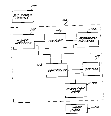
Figure 1 is a block diagram of an induction
heater constructed according to one aspect of the present
invention;
Figure 2 is a circuit diagram of the power
inverter shown in Figure l; and
Figure 3 is a circuit diagram of the frequency
inverter shown in Figure 1.
D~TAILED DESCRIPTIO~ OF A PR~FERRED EXENPhARY EMBODIMENT
Before explaining at least one embodiment of
the invention in detail it is to be understood that the
invention is not limited in its application to the
details of construction and the arrangement of the
components set forth in the following description or
illustrated in the drawings. The invention is capable of
othèr embodiments or being practiced or carried out in
various ways. Also, it is to be understood that the
phraseology and terminology employed herein is for the
purposes of description and should not be regarded as
limiting.
The present invention relates to an induction
heater such as one used to cure an adhesive for adhering
a piece of metal to another object. The illustrated
induction heater is constructed to provide peak power ~ `
independent of operating frequency and is further capable
of utilizing a DC input or an AC input.
- . . . ~ .
w093t04s66 PCT/US92/~9ss
2 ~ 93 139 -6-
Referring to Figure 1 an induction heater,
designated generally as 100, includes a power inverter
102, a frequency inverter 104, an induction head 106, a
controller 108, and couplers 110 and 112. Also shown in
Figure 1 is a workpiece 116, which induction heater loo
heats, and a DC power source 114.
In operation, power inverter 102 receives DC
power from DC power source 114. Alternatively, the power
source may be an AC power source, and a rectifier may be
provided, so that power inverter 102 receives a rectified
AC power supply. Power inverter 102 then inverts the DC
power supply signal, and pulse width modulates the
inverted signal (also called phase modulation or control
of the inverter signal), to provide an AC signal at a
first frequency that is high enough to respond quickly to
feedback signals, but not so fast as to cause stress to
the inverter components. Coupler llo then rectifies the
AC signal to provide a second DC signal having a
magnitude dependent upon the pulse width or phase
modulation of the AC signal power inverter 102.
The second DC signal, the output of coupler
110, is applied to frequency inverter 104. Fre~uency
inverter 104 inverts the DC signal at a user-selectable
frequency selected to optimi~e heating. The magnitude of
the AC signal is dependent upon the magnitude of the DC
input signal, and is thus responsive to the pulse width
modulation of power inverter 102. The AC signal is
transformed by coupler 112 and is applied to induction
head 106.
The AC current through induction head 106
induces current in workpiece 116, thus causing workpiece
116 to become hot at the location near induction head
106. Peak heat intensity produced in workpiece 116 is
dependent upon the peak magnetic flux induced in the
workpiece. The magnetic flux in turn is responsive to
:,
, , , ': ` '~ ' ,
wO 93/04566 PCI/US92/069S9
2~93139
--7--
the magnitude of the signal provide by frequency inverter
104, and thus also is responsive to the phase modulation
of power inverter 102. Controller 108 is provided to
sontrol the pulse width modulation of power inverter 102,
5 and the frequency of operation of frequency inverter 104.
Referring now to Figure 2, power inverter 102
is shown along with a three phase rectifier 202. Power
inverter 102 is shown to include a plurality of MOSFETs
Ql-Q4, a plurality of capacitors Cl-ClO, a plurality of
10 diodes Dl-D8, a plurality of resistors R1-R7 and an
inductor Ll. A transformer Tl, which is part of coupler
110, is also shown. In operation three phase rectifier
202 preferably provides up to 100 amps at 1200 volts by ; ..
rectifying a 460 volt, three phase AC signal.
In general there are two mutually exclusive
cur-ent paths for providing current f}ow first in one
direction thr~ugh the primary transformer Tl and then in
the opposite direction through the primary of transformer
Tl. The current paths are: first, from the positive
output of three phase rectifier 202 through MOSFET Ql,
capacitor C5, the primary of transformer Tl, MOSFET Q4,
and back to the negative output of the rectifier; and,
second, from capacitor C5, through MOSFET Q2, MOSFET Q3,
the primary of transformer Tl, and back to capacitor C5.
These paths are selected by turning MOSFETs Ql and Q4 on
and MOSFETs Q2 and Q3 off, or conversely, by turning
MOSFETs Q2 and Q3 on and MOSFETs Q1 and Q4 off. :
In operation capacitor C5 is charged to about
325 volts, or one half of the 650 volt supply. Thus, .:
when MOSFETs Ql and Q4 are on, ignoring voltage drops
across MOSFETs Q4 ànd Ql, approximately 325 volts (650
volt supply minus 325 volts across capacitor ~5) is
applied to the primary of transformer Tl, with the upper
terminal of the primary being positive with respect to
the lower terminal. ~:
~,..... ............................................................ ..~.
:
- .: ,
.
,~ , .
., .
w093/04~66 PCT/US92/06959
2~93~39 -
When MOSFETs Q2 and Q3 are on and MOSFETs Ql
and Q4 are off, approximately 325 volts is applied across
the primary of transformer Tl in the opposite direction.
Capacitors C6-Cs are provided to tie the voltage between
MOSFETs Q2 and Q3 to 325 volts, or one-half of the
rectified input. When MOSFETs Q2 and Q3 are on, the
voltage between MOSFET Q2 and capacitor C5 is tied to the
voltage at the node common to MOSFETs Q2 and Q3 and
capacitors C6-Cs, or about 325 volts. The voltage across
capacitor ~5, which is an 8 microfarad high current
polypropylene capacitor, is 325 volts, and due to the
large capacitance of capacitor C5, will not change `
quickly. Thus, the voltage applied to the top of the
primary of transformer Tl is 2ero volts. Also, through
MOSFET Q3 and capacitors C6-C9, 325 volts is applied to
the bottom of the primary of transformer Tl. Thus,
turning MOSFETs Q2 and Q3 on causes 325 volts to be
applied to transformer Tl, but in the reverse direction
of the 325 volts applied by turning on MOSFETs Ql and Q4.
In order to pulse width modulate, or phase
control, the signal applied to the primary of transformer
Tl, MOSFETs Ql and Q2 are turned on and off at a constant
frequency, preferably about 50 kilohertz. MOSFETs Ql and `
Q2 are 180 degrees out of phase, and each has a duty
cycle of 50%. MOSFETs Q3 and Q4 also have duty cycles of
50% and are 180 degrees out of phase from one another.
Also, MOSFETs Q3 and Q4 are slaved to MOSFETs Q2 and Ql,
respectively, in that they may be turned on from zero to
180 degrees out of phase with respect to the respective
time MOSFETs Ql and Q2 are on. Because a pulse is
applied to the primary of transformer Tl only when both
MOSFETs Q1 and Q4 are on, or when both MOSFETs Q2 and Q3
are on, the phase of MOSFET Q4 relative to MOSFET Ql, and
the phase of MOSFET Q3 relative to MOSFET Q2, determines
the pulse width of the signal applied to the primary of
, . , , -
:; :
W093/04566 PCT/US92/06959
2093139
transformer T1. Because MOSFETs Q3 and Q4 are 180
degrees out of phase of one another, they are each out of
phase with respect to MOSFETs Q2 and Ql, respectively, by
an identical amount.
For example, when MOSFET Q3 is zero deqrees out
of phase with respect to (in phase with) NOSFET Q2,
MOSFET Q3 will be on the entire half cycle that MOSFET Q2
is on, and a pulse for the full half cycle will be
applied to the primary o~ transformer Tl. Also, if
MOSFET Q3 is in phase with MOSFET Q2, then MOSFET Q4 will
be in phase with MOSFET Ql, and a pulse for the full
other half cycle will also be provided to the primary of
transformer Tl. Conversely, when MOSFET Q3 is 180
degrees out of phase with respect to MOSFET Q2, MOSFET Q3
will be off the entire half cycle that MOSFET Q2 is on,
and no pulse will be applied to the primary of
transformer Tl. Again, MOSFET Q4 will also be 180
degrees out of phase with respect to MOSFET Ql, and no
pulse will be provided on the other half cycle.
In general, because MOSFET Q3 is out of phase with
respect to MOSFET Q2 by the same amount that MOSFET Q4 is
out of phase with respect to MOSFET Q1, in steady state `~
operation the opposite polarity pulses will have the same -
width. Thus, the width of the 325 volt pulses applied to :
the primary of transformer Tl is dependent upon the phase
of MOSFET Q4 with respect to MOSFET Q1, and the phase of
MOSFET Q3 with respect to MOSFET Q2.
Accordingly, to control the total current
output of power inverter 102, controller 108, which may
include a conventional pulse width modulator, applies ~
signals to the gates of MOSFETs Ql-Q4 and controls the ~-:
phase of NOSFETs Q3 and Q4 with respect to MOSFETs Q2 and
Q1. Alternatively, controller 108 may include a
plurality of timers such as a CMOS 4098 dual timer,
available from Harris Semiconductor, and a flip-flop, to
. .
. . . .
~ . ~
~. - ,.'. ~ .
.. . .
.: ~
w093/04566 PCT/US92/06959
2393~39
--10-- .
provide the control of MOSFETS Ql and Q2. To provide the
control of MOSFETS Q3 and Q4, which are slaved to Q2 and
Ql, a comparator may be used, having its output connected
to a flip-flop and having as inputs a ramp generator and
a signal having a magnitude dependent on the desired
phase difference between MOSFETS Ql/Q2, and Q4/Q3. Thus,
a pulse may be narrow or wide, even though in steady
state operation all MOSFETs have a 50~ duty cycle, to
help insure that high heat build up does not occur in
MOSFETs Ql-Q4, to protect the components. It may be
desirable to provide a deadband, wherein, for example,
the turning on of Ql or Q3, is delayed slightly from the
turning off of Q2 or Q4, respectively, so that Q2 or Q4
will be completely off before Ql or Q3 is on.
Capacitors Cl-C4 are small polypropylene
snubbing capacitors and diodes Dl-D6 and resistors R5 and
R6 are provided to protect MOSFETs Ql-Q4. Capacitors C6
and C8 are large electrolytic capacitors, typically 1700
microfarads and split the voltage provided by three phase
rectifier 202 to one-half of the supply voltage at the
node common to MOSFETs Q2 and Q3. Capacitors C7 and C9
are 8 microfarad high current polypropylene capacitors,
provided to smooth the voltage seen by the node common to
MOSFETs Q2 and Q3. Diodes D7 and D8 and resistor R7 and
inductor Ll, along with capacitor C10 are provided to
prevent unbalancing of the node common to MOSFETs Q2 and
Q3. Specifically~ when capacitors C6 and C7 have a
voltage across them other than that of capacitors C~ and
C9, inductor Ll acts as a spillover inductor and causes
the voltage across capacitors C6 and C7 to become equal
to that across capacitors C8 and C9. Resistors R1-R4
protect the gate of MOSFETs Ql-Q4.
Referring now to Figure 3 coupler 110,
frequency inverter 104, coupler 112 and induction head
106 are shown. Coupler 110 includes transformer Tl, a
w093/04s66 2 0 9 ~ 1 3 9 PCT/US92/06~9
plurality of diodes D9-D12, a voltage regulator VR1, and
a capacitor Cll.
The primary of transformer Tl is connected to
the output of power inverter 102. As described above,
the primary of transformer Tl receives a pulse width
modulated AC signal at a desired frequency, exemplified
herein to be about 50 Khz. The width of the pulses is
determined by phase controller 108 as described above.
The secondary of transformer Tl is connected to a diode
bridge comprised of diodes D9-D12, which rectifies the AC
signal. The rectified signal is applied to capacitor Cll
causing a voltage across it. Voltage regulator VRl is
provided to ensure that the voltage across capacitor Cll
is not greater than a predetermined limit, selected to
lS protect the components of the inverter. The voltage
across capacitor Cll is directly responsive to the total
current induced in the secondary of transformer Tl, which
is responsive to the width of the pulses qenerated by
power inverter 102. The DC voltage across capacitor Cll
is provided as the DC input to frequency inverter 104.
Frequency inverter 104 may be a conventional
inverter operable at a user adjustable frequency of,
e.g., between lo kHz and 1 MHz, but preferably between 25
kHz and So kHz. The frequency range may be higher or
lower, depending on the required usè of the induction
heater. Accordingly, frequency inverter 104 may include
transistors Q10-Q13 and capacitors C12-C17. Transistors
Q10 and Q12 are turned on and off in unison and
transistors Qll and Q13 are turned on and off in unison.
Moreover, whenever transistors Q10 and Q12 are on
transistors Qll and Q13 will be off. It may be necessary
to provide a dead band wh`erein, before turning on one `
pair of transistors, the other pair is allowed to turn
off. Controller 108 provides the appropriate on and off
signals to the gates of transistors Q10-Q13. Capacitors j;
~, ~
, ,:
. , .
. :. . . ..
w093t~566 PCT/US92t~9S9
2093~39 -12-
C12 and C15-C17 are provided to eliminate switching
losses when transistors Q10-Q13 are switched off.
Capacitors C13 and C14 are provided to block DC current
through an output transformer T3, to prevent saturation
of transformer T3.
The output of frequency inverter 104 is
provided to coupler 112. Coupler 112 includes a current
feedback device 301, which is a ferrite toroidal core
with a sixty turn secondary and a single turn primary.
The single turn primary is connected to the primary of
transformer T3. The output of current feedback device
301 is provided to controller 108 w~ich adjusts the pulse
width of power inverter 102 in a conventional manner. In
addition to the current feedback, a voltage feedback may
lS be provided to controller 108. Controller 108 may then
determine the power (voltage multiplied by current)
delivered to induction head 106. Controller 108 may also
determine the heat lost in the induction head 106 due to
the resistance of the induction head, which will be the
current squared, multiplied by the resistance of
induction head 106. The difference between the power
delivered and the power lost in the induction head is
egual to the power delivered to workpiece 116. The
multiplication may be carried out using known multiplier
2S chips such as an MPY634 KP chip available from Burr
Brown, and the subtraction may be carried out with an op
amp. The output of frequency inverter 104 is provided
through a primary winding on transformer T3, which may
preferably be a coaxial transformer, and induces a
current in a secondary winding of transformer T3 which is
preferably a two turn loop applied to induction head 106.
Accordingly, as frequency inverter 104 drives current
through the primary of transformer T3 at the user
selectable frequency, a current of the same frequency is
,.~. -
. .
w093/04566 2 0 9 ~ 1 3 9 PCT/US92/06959
induced in induction head 106, thereby heating workpiece
116.
Other modifications may be made in the design
and arrangement of the elements discussed herein without
departing from the spirit and scope of the invention, as
expressed in the appended claims.
- ,. . .. : . . -
. .
,, ........... ~. . - . , . -
-.......... . . - : ~ . .-~ . -