Note : Les descriptions sont présentées dans la langue officielle dans laquelle elles ont été soumises.
~
,_ \
~~~.~~~.'~
SPECIFICATION
TITLE OF THE INVENTION
DIELECTRIC FILTERS AND DUPLEXERS INCORPORATING
SAME
FIELD OF INDUSTRICAL APPLICATION
The present invention relates to dielectric
filters for use in mobile communication systems for the
microwave band, and duplexers having such filters
incorporated therein for use in radio devices.
PRIOR ART
Conventinal dielectric filters wherein coaxial
resonators are used include, for example, the one
disclosed in Examined Japanese Utility Model Publica-
tion No. 44566/1987 (FIG. 28). The disclosed dielectric
filter comprises a plurality of quarter-wavelength
coaxial resonators 1 each including a dielectric member
12 which has a through hole 4. The outer peripheral
surface of the dielectric member and the inner peripheral
surface thereof defining the through hole are covered
with an electrically conductive material to provide an
outer conductor 5 and an inner conductor 6, respectively.
The dielectric member has an open end face la where the
outer conductor 5 and the inner conductor 6 each have
a free end, and a short-circuit end face lb where the
r~
a
the other ends of the conductors are short-circuited.
A connecting member comprising a dielectric
bush 14 and a connecting bar 15 is fitted in the through
hole 4 of each coaxial resonator 1, and the other end
of the bar 15 is joined to a coupling electrode 13 on a
substrate 16, whereby the dielectric filter is
capacitance-coupled to an external circuit.
It has been required in recent years that
mobile communication devices be made smaller in size
and lightweight. To comply with this requirement,
the dielectric filter, one of the components of these
devices, also need to be compacted.
In providing compacted dielectric filters,
the ratio of the inner conductor 6 to the outer conductor
5 in diameter must be 3.6 in order to obtain a high Qu
value (no-loaded Q factor). If the diameter of the
outer conductor 5 is up to 4 mm, the diameter of the
inner conductor 6 is up to 1.1 mm, whereas extreme
difficulties are encountered in the prior art in
inserting the connecting members 14, 15 into the through
hole 4 of the coaxial resonator for connection to the
external circuit 13. Thus, compacting the dielectric
filter is limited.
In mobile communication devices, on the other
hand, signals of different frequencies are separated
_2_
~~~~~ ~~.s~
according to the frequency or are combined together
using duplexers. Such duplexers comprise a transmitting
dielectric filter and a receiving dielectric filter
which are different in center frequency. With the trend
of mobile communication toward higher frequencies, the
difference between the receiving band and the transmit-
ting band in center frequency becomes smaller, making
it difficult for these dielectric filters to attain
the desired attenuation outside the pass band. Accord-
ingly, the characteristics of the dielectric filters
for use in the duplexer must involve a local minimum
of attenuation.
The present applicant filed a patent applica-
tion with the Patent Office of Japan for a dielectric
filter which is free of the above problem and which
has the construction shown in FIG. 29 (Japanese Patent
Application No. 46796/1991). A U.S. patent has been
granted for the filter as No. 5,144,269.
This dielectric filter comprises a plurality
of coaxial resonators 1 arranged side by side and each
having a dielectric member 12 formed with a through
hole 4. The outer and inner peripheral surfaces of the
dielectric member 12 are covered with a conductive
material to provide an outer conductor 5 and an inner
conductor 6, respectively. The resonator has a short-
-3-
circuit end face and an open end face, in the vicinity
of which the outer conductor 6 is partially removed,
along with a portion of the dielectric member when so
desired, to form a recess 17. A dielectric substrate
19 provided with an external connection electride 18
is attached to the recessed portion 17.
At least three coaxial resonators are used
in the filter to provide a local minimum of attenua-
tion. More specifically, a capacitance is formed
between the external connection electrode 18 and a
capacitance-forming electrode provided on the dielectric
substrate 19 to obtain frequency characteristics
involving a local minimum in the attenuation region.
With the filter described above, however,
the resonator needs machining for forming the recessed
portion 17 for attaching the dielectric substrate
thereto and therefore can not be compacted without
limitations. The characteristics of the filter also
have the problem that sufficient suppression is not
available outside the pass band.
The dielectric filter has another problem
in that the coaxial resonator can not be reduced in its
overall length because the substrate 19 needs to be
partly projected from the dielectric member 12 for
coupling to an external circuit.
-4-
.~'\
G
SUMMARY OF THE INVENTION
The present invention provides a dielectric
filter of reduced size which comprises a substrate
having approximately the same shape and area as the
bottom contour of an arrangement of coaxial resonators
and wherein the arrangement of resonators is mounted
on the substrate in register therewith without permitting
the substrate to project beyond the resonators.
An object of the present invention is to
provide a dielectric filter which is reduced in size
and which has excellent characteristics involving a
local minimum of attenuation to attain the desired
attenuation outside the pass band.
Another object of the invention is to provide a
duplexer comprising such dielectric filters as
transmitting and receiving filters.
The present invention provides a dielectric
filter which is characterized in that the filter comprises
a dielectric substrate having input and output coupling strip
lines on a surface thereof, and a plurality of coaxial
resonators, each of the resonators comprising a
dielectric member having a through hole, an outer peri-
pheral surface and an inner peripheral surface, the outer
and inner peripheral surfaces being covered with an
electrically conductive material to provide an outer
-5-
CA 02093312 2000-06-07
conductor and an inner conductor, respectively, the
outer conductor being partially removed, the plurality
of coaxial resonators including an input resonator and
an output resonator arranged on the dielectric substrate
with open end faces thereof oriented in directions
opposite to each other, the dielectric substrate being
shaped in conformity with the bottom contour of the
plurality of coaxial resonators as arranged on the
substrate.
The present invention also provides a duplexer
which comprises a receiving filter and a transmitting
filter each comprising three coaxial resonators serving
respectively as an input stage, an output stage and an
intermediate stage, each of the resonators having the
above construction, and a dielectric substrate provided
with input and output coupling strip lines for
transmitting therethrough inputs and outputs of the
coaxial resonators and with a receiving matching circuit
and a transmitting matching circuit for connecting the
receiving filter and the transmitting filter to one
antenna.
Accordingly, in one aspect, the present
invention provides a dielectric filter comprising: a
dielectric substrate having input and output coupling
strip lines, and a plurality of coaxial resonators, each
of the resonators comprising a dielectric member having
-6-
CA 02093312 2000-06-07
a through hole, an outer peripheral surface and an inner
peripheral surface, the outer and inner peripheral
surfaces being covered with an electrically conductive
material to provide an outer conductor and an inner
conductor respectively, the outer conductor being
partially removed, the resonator having an end face
where the outer and inner conductors are short-circuited
and an open end face where the outer and inner
conductors are not connected to each other, the
plurality of coaxial resonators including a pair of
resonators serving as an input stage and an output stage
and arranged on the dielectric substrate with their open
end faces oriented in directions opposite to each other,
the dielectric substrate being shaped in the dimensions
of width and length substantially in conformity with a
bottom contour of the plurality of resonators as
arranged on the substrate; and wherein said pair of
resonators serving as an input stage and an output stage
are coupled to the input and output coupling strip
lines, respectively.
In a still further aspect, the present
invention provides a dielectric filter comprising: a
dielectric substrate having input and output coupling
strip lines, and a plurality of coaxial resonators, each
of the resonators comprising a dielectric member having
a through hole, an outer peripheral surface and an inner
CA 02093312 2000-06-07
peripheral surface, the outer and inner peripheral
surfaces being covered with an electrically conductive
material to provide an outer conductor and an inner
conductor respectively, the outer conductor being
partially removed, the resonator having an end face
where the outer and inner conductors are short-circuited
and an open end face where the outer and inner
conductors are not connected to each other, the input
and output coupling strip lines extend in parallel to
each other from one side of the dielectric substrate
toward the same direction, the plurality of coaxial
resonators including resonators serving as an input
stage and an output stage and arranged on the dielectric
substrate with their open end faces oriented toward the
side of the dielectric substrate having the strip lines,
the plurality of coaxial resonators including a coaxial
resonator of an intermediate stage having its open end
face oriented in a direction opposite to the open end
faces of the resonators of the input and output stages,
each of the resonators being mounted on the dielectric
substrate, the dielectric substrate being shaped in the
dimensions of width and length substantially in
conformity with a bottom contour of the plurality of
resonators as arranged on the substrate; and wherein the
resonators serving as an input stage and an output stage
-7a-
CA 02093312 2000-06-07
are coupled to the input and output coupling strip
lines, respectively.
BRIEF DESCRIPTION OF THE DRAWINGS
FIG. 1 is a perspective view showing a first
embodiment of dielectric filter;
FIG. lA is a view in section taken along the
line X-X in FIG. 1;
FIG. 2 is a perspective view showing coaxial
resonators for use in the invention;
FIG. 3 is a plan view showing the first
embodiment of dielectric filter;
FIG. 4, (A) to (D) are projection drawings of
different surfaces of a dielectric substrate for use in
the first embodiment;
FIG. 5 is an equivalent circuit diagram of the
first embodiment;
FIG. 6 is a graph showing the filter
characteristics of the first embodiment;
FIG. 7 is a graph showing higher-order pass
band characteristics of the first embodiment;
FIG. 8, (A) to (D) are projection drawings of
different surfaces of a dielectric substrate for use in
a second embodiment;
FIG. 9 is a plan view showing dielectric
substrates while they are being prepared for use in the
second embodiment;
-7b-
CA 02093312 2000-06-07
FIG. 10 is a view showing a cover for use in
the second embodiment;
FIG. 11 is an exploded perspective view
showing the components to be assembled into the second
embodiment;
FIG. 12 is a perspective view showing the
second embodiment;
FIG. 13, (A) to (D) are projection drawings
-7c-
='"'\
~. . ,: y, :: S ~ -:;1
showing different surfaces of a dielectric substrate
for use in a third embodiment;
FIG. 14, (A) to (D) are projection drawings
showing different surfaces of a dielectric substrate
for use in a fourth embodiment;
FIG. 15 is an equivalent circuit diagram of
the third and fourth embodiments;
FIG. 16 is a graph showing the filter
characteristics of the first, second, third and fourth
embodiments;
FIG. 17 is a perspective view of a fifth
embodiment;
FIG. 18, (A) to (D) are projetion drawings
showing different surfaces of a dielectric substrate
for use in the fifth embodiment;
FIG. 19 is an equivalent circuit diagram of
the fifth embodiment;
FIG. 20 is a graph showing the filter
characteristics of the fifth embodiment;
FIG. 21 is a perspective view showing a sixth
embodiment;
FIG. 22, (A) to (D) are projection drawings
showing different surfaces of a dielectric substrate
for use in the sixth embodiment;
FIG. 23 is an equivalent circuit diagram
_g_
of the sixth embodiment;
FIG. 24 is a graph showing the filter
characteristics of the sixth embodiment;
FIG. 25 is a view showing a duplexer as a
seventh embodiment;
FIG. 26 is a plan view showing a dielectric
substrate for use in the duplexer;
FIG. 27 is an equivalent circuit diagram
schematically showing the duplexer;
FIG. 28 is a sectional view of a convention-
al dielectric filter; and
FIG. 29 is a perspective view of a dielectric
filter already filed for application by the present
inventors.
DETAILED DESCRIPTION OF THE INVENTION
First Embodiment
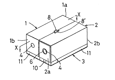
FIGS. 1 to 7 show a dielectric filter of the
invention, i.e., a first embodiment, which comprises
two coaxial resonators 1, 2 and a dielectric substrate 3.
Each of the two coaxial resonators 1, 2 is a
quarter-wavelength coaxial resonator, which comprises,
as shown in FIG. 2, a dielectric member 12 in the form
of a prism and having a through hole 4. The outer and
inner peripheral surfaces of the dielectric member 12
are covered with silver or like electrically conductive
_g_
~~9~~ ~.
material to provide an outer conductor 5 and an inner
conductor 6, respectively. One end face of the
resonator is covered with the conductive material to
provide a short-circuit end face lb where the outer and
inner conductors 5, 6 are short-circuited. The
dielectric member is left exposed at the other end face
of the resonator to provide an open end face la. The
two resonators l, 2 are arranged side by side and joined
together by soldering, with their open end faces
oriented in directions opposite to each other. The
outer conductor is removed from the bottom of the
assembly to form a bottom portion 7.
Each of the coaxial resonators 1, 2 is adapted
for use with frequencies in the range of several
hundreds of MHz to 3 GHz. The resonator has a square
cross section measuring slightly less than 2.0 mm in
each side, is 0.7 mm in the diameter of the through hole
4 and has a length which is 4.2 mm when it is used for
a frequency of 1.9 GHz.
The two coaxial resonators 1, 2 are formed in
the center of their adjacent surfaces with interstage cou-
pling windows 8, 8' respectively by removing the outer
conductors 5 perpendicular to the direction of the through
holes 4. As shown in FIG. 3, the windows 8 and 8' have
widths W and W', respectively, which are different
-10-
from each other. Accordingly, even if the two resona-
tors 1, 2 are joined together by soldering as slightly
displaced from each other, the assembly has a definite
effective interstage coupling width, and the degree of
coupling will not vary from product to product.
The coaxial resonators 1, 2 are placed on the
dielectric substrate 3 with the bottom portion 7 down
and with their open end faces la, 2a oriented in
directions opposite to each other.
FIG. 4 shows the dielectric substrate 3.
FIG. 4, (A) shows the front surface of the substrate,
FIG. 4, (B) the rear surface thereof, and FIG. 4, (C)
and (D) side faces thereof.
The substrate 3 has approximately the same
shape and area as the contour of the bottom portion 7
of assembly of the two resonators 1, 2 as arranged side
by side as shown in FIG. 1. Input and output coupling
strip lines 9, 10 are formed on the front and rear
surfaces of the dielectric substrate 3, whereby the
resonators 1, 2 are connected to an external circuit
for input-output coupling. Indicated at 11 is a grounding
electrode extending along the side end faces of the
substrate 3 to electrically connect the front surface to
the rear surface, and is provided around the input
coupling strip line 9 and the output coupling strip line
-11-
to prevent electrical interference between the strip
lines 9, 10.
As shown in FIG. 1, the resonators 1, 2 have
their open end faces la, 2a positioned on the input
5 and output coupling strip lines 9, 10, respectively, and
are affixed to the dielectric substrate 3 with an epoxy
or like adhesive. The outer conductors 5 of the
resonators 1, 2 are thereafter soldered to the grounding
electrode 11 on the substrate 3. Thus, the dielectric
10 filter is completed.
The dielectric filter thus constructed is
shown in FIG. 5 as an equivalent circuit. Capacitances
C1, C2 are formed between the inner conductors 6 of
the coaxial resonators 1, 2 and the respective input and
output coupling strip lines 9, 10 for capacitance
coupling. A capacitance C3 is formed by the inner ,
conductors 6, 6 of the resonators 1, 2 owing to the
presence of the interstage coupling windows 8, 8' for
capacitance coupling, whereby a filter is provided.
The filter characteristics of this embodiment are shown
in FIG. 6.
The dielectric substrate 3 has approximately
the same area and contour as the bottom portion of
assembly of the two coaxial resonators 1, 2 and does
not have the portion 15 greatly projecting outward
-12-
~~~3312
unlike the conventional filter (FIG. 28). When
incorporating the present filter, communication devices
can therefore be made smaller in size.
FIG. 7 shows the higher-order pass band
characteristics of the present embodiment. The solid
line represents the dielectric filter of the invention,
and the broken line the prior-art device (FIG. 28).
According to the present invention, coaxial resonators
serving as an input stage and an output stage are
arranged on a dielectric substrate with their open end
faces spaced apart as oriented in opposite directions.
This eliminates matching at 3 fo and 5 fo owing to
variations in higher-order frequency, affording improved
ability to suppresss waves other than the dominant
wave.
Second Embodiment
FIGS. 8 to 12 show a second embodiment of
the invention which also comprises the coaxial resona-
tors~l, 2 shown in FIG. 2.
The dielectric substrate 3 to be used in the
present embodiment is shown in FIG. 8. The front surface
of the substrate for placing the resonators 1, 2 thereon
is shown in FIG. 8, (A), the rear surface thereof in
FIG. 8, (B) and side faces thereof in FIG. 8, (C) and
(D). The dielectric substrate 3 has approximately the
-13-
shape and area as the contour of the bottom portion of
arrangement of the two coaxial resonators 1, 2.
Indicated at 9, 10 are input and output coupling strip
lines, through which the resonators 1, 2 are connected
to an external circuit for input-output coupling.
Indicated at 11 is a grounding electrode provided on
the resonator bearing surface of the substrate formed
with the stip lines 9, 10 so as to surround these strip
lines 9, 10. The electrode 11 is electrically
connected to a grounding electrode formed approximately
over the entire rear surface of the substrate, on the
front and rear surfaces by means of through holes 23
and through holes 24. The electrode 11 also serves to
obviate electrical interference between the input
coupling strip line 9 and the output coupling strip
line 10. Each of the input and output coupling strip
lines 9, 10 is electrically connected to a corresponding
one on the rear surface by a through hole 25.
FIG. 9 shows the front surface of dielectric
substrates 3, 3 in the course of preparation. These
substrates 3, 3 are formed by printing input and output
strip lines 9, 10 and grounding electrode 11 on each
of opposite surfaces of a substrate blank 26 of
dielectric material, printing a grounding electrode on
the rear surface of the blank 26. forming through holes
-14-
z3 :~
23 and 24 for connection and through holes 25 for
inputting and outputting in the blank 26, and cutting
the blank along the broken lines shown in the drawing.
FIG. 10 shows an electrically conductive cover
27, which is prepared by blanking out a piece of the
illustrated configuration from a conductive member and
thereafter bending the piece along the broken lines
shown. The conductive cover 27 has a plurality of
connecting end portions 28 resembling comb teeth and
formed at each of its opposite ends by blanking, and
an interstage coupling degree adjusting window 29 and
soldering windows 30 formed approximately at the center
of the cover by punching. The pitch P of the connecting
end portions 28 is equal to the pitch of the through
holes 23 in the dielectric substrate. The end portions
28 have a width W" which is equal to or slightly smaller
than the diameter of the through holes 23. Suitable as
the material of the conductive member is copper or like
material having high conductivity, while in view of
the coefficient of expansion and strength, it is suitable
to use a copper alloy. The material is most suitably
a copper alloy comprising up to 0.2 wt. $ of Fe, up to
0.1 wt. $ of P, up to 1.0 wt. $ of Sn and the balance
Cu.
The second embodiment of the invention is
-15-
~~~~J~~
assembled in the manner to be described below with
reference to FIG. 11. The coaxial resonators 1, 2 are
arranged with their open end faces la, 2a oriented in
directions opposite to each other and with these faces
la, 2a lapping over the respective input and output
coupling strip lines 9, 10. The bottom portion 7 of
the arrangement is affixed to the dielectric substrate
3 with an epoxy resin or like adhesive, with a cream
solder applied to the outer conductors 5 of the two
resonators 1, 2.
The conductive cover 27 is then placed over
the resonators l, 2. At this time, the connecting end
portions 28 fit into the through holes 23 in the sub-
strate 3 and are temporarily fixed in position. The
resulting assembly is then heated in a reflow oven
and soldered with the cream solder applied. This
procedure electrically connects the outer conductors 5
of the resonators 1, 2 to the cover 27 and the end
portions 28 of the cover 27 to the through holes
23 to connect the outer conductors 5 of the resona-
tors 1, 2 to the grounding electrodes 11, 11 of the
substrate 3.
The interstage coupling window 8 is thereafter
trimmed with a diamond bar or the like through the
coupling degree adjusting window 29 formed in the cover
-16-
r.~\
27 to thereby adjust the pass band characteristics.
Finally, a seal member 31 is affixed to the cover 27
to assure the filter of reliability. If a material
having an aluminum or like metal layer formed by vacuum
evaporation is used as the seal member, a leakage
magnetic field will penetrate through the seal member
to entail an increased energy loss, which results in
problems such as an increased insertion loss and
variations in the center frequency. It is therefore
desired to use resin, paper or like insulating material
for the seal member 31.
With the dielectric filter of the present
embodiment, the outer conductors of the coaxial resona-
tors serving as an input stage and an output stage are
electrically connected to the grounding electrode
via the comb-toothed connecting end portions of the
cover and through holes in the dielectric substrate,
so that the resonators can be connected to the substrate
with good stability, assuring the filter of high
performance free of variations in its characteristics
and impairment of the characteristics due to variations
in the grounding condition.
Third and Fourth Embodiments
FIGS. 13 and 14 show other dielectric filters
of the invention, i.e., third and fourth embodiments,
-17-
'~~9F~'~~'~
respectively. More specifically, each of these drawings
shows the dielectric substrate 3 to be used in the
embodiment. Throughout FIGS. 8, 13 and 14, like parts
are designated by like reference numerals and will not
be described again. In FIGS. 13 and 14, (A) shows
the front surface for placing coaxial resonators 1, 2
on, (B) shows the rear surface, and (C) and (D) show
side faces.
With the third embodiment shown in FIG. 13, a
grounding electrode 11 provided so as to surround the
input and output coupling strip lines 9, 10 is electri-
cally connected to a grounding electrode 11 formed
approximately over the entire rear surface of the
dielectric substrate 3 by means of a plurality of
through holes 23 formed in each of right and left
opposite side faces of the substrate 3 where the strip
lines 9, 10 are not formed.
With the fourth embodiment shown in FIG. 14,
a grounding electrode 11 provided around the input and
output coupling strip lines 9, 10 is electrically
connected to a grounding electrode 11 formed approxi-
mately over the entire rear surface of the dielectric
substrate 3 by means of through holes 23 formed in the
right and left opposite side faces of the substrate 3
having neither of the strip lines 9, 10 and also by means
-18-
of a through hole 36 formed in one of the front and
rear side faces having the input and output coupling
strip lines 9, 10, respectively.
Each of these dielectric substrates thus
obtained is used to assemble a dielectric filter like
the second embodiment shown in FIG. 11.
FIG. 15 shows an equivalent circuit diagram
of the dielectric filters thus constructed. Indicated
at C4 and C5 are coupling capacitances formed between
the inner conductors of the coaxial resonators 1, 2
and the respective input and output coupling strip lines
9, 10 on the dielectric substrate 3. Indicated at C6
is a coupling capacitance between the coaxial resonators
provided by the interstage coupling window 8 formed
in the resonators 1, 2, and at C7 is a coupling
capacitance formed between the outer conductors 5 of
the resonators 1, 2 and the grounding electrode 11
on the rear surface of the substrate 3. The value of
C7 is dependent on the strength of electrical coupling
between the outer conductors 5 of the resonators 1, 2
and the rear grounding electrode 11 on the substrate 3,
i.e., the presence or absence of the through holes 23
and 36, whereby the characteristics of the dielectric
filter is made to have a local minimum of attenuation.
FIG. 16 shows the filter characteristics of
-19-
/ '~
dielectric filters of the present invention. With
reference to the drawing, A respresents the case wherein
the dielectric substrate 3 of the third embodiment
FIG. 13) is used, the substrate 3 having the through
holes 23 only in the right and left opposite side
faces thereof. B represents the case wherein the
dielectric substrate 3 of the fourth embodiment (FIG.
14) is used, the substrate having, in addition to the
through holes 23, the through hole 36 formed in one
of the front and rear side faces having the strip lines
9, 10 respectively. C represents the characteristics
of the first embodiment shown in FIG. 1 and the second
embodiment shown in FIG. 12. Reliable electrical
coupling is achieved between the outer conductors 5 of
the coaxial resonators 1, 2 and the rear grounding
electrode 11 on the substrate.
As represented by A and B in FIG. 16, the
position of local minimum in the attenuation region is
controllable according to the strength of electrical
coupling between the resonator outer conductors 5 and
the rear grounding electrode 11 on the dielectric
substrate 3, i.e., according to presence or absence
of the through hole 36 in one of the front and rear
side faces having the strip lines 9. 10.
Fifth Embodiment
-20-
~~3~'~ ~.
FIG. 17 shows a fifth embodiment of the
present invention which comprises three coaxial resona-
tors, i.e., coaxial resonoators 1, 2 of input and output
stages, and a coaxial resonators 37 of intermediate
stage interposed between the resonators 1, 2. The
resonators 1, 2 and 37 are arranged on a dielectric
substrate 3. As shown in FIG. 18, the substrate 3 has
a grounding electrode or pattern 11 surrounding input
and output coupling strip lines 9, 10 and electrically
connected at side faces of the substrate to a grounding
pattern 11 formed substantially over the entire rear
surface of the substrate. Alternatively, these ground-
ing patterns 11, 11 may be connected together by means
of through holes as in the second embodiment shown in
FIG. 8. The input and output coupling strip lines 9, 10
extend from one side of the dielectric substrate 3
toward one direction. Indicated at 42 is a resonator
length correcting strip line for making the length of
the resonator 37 of intermediate stage to that of the
resonators 1, 2 of input and output stages. The coaxial
resonators 1, 37 and 2 are arranged as oriented
alternately in opposite directions. The resonators are
first fixed onto the substrate 3 with an adhesive, and
the outer conductors are thereafter soldered to the
grounding electrode 11 on the substrate 3 for electrical
-21-
--,
connection.
FIG. 19 is an equivalent circuit diagram of
the fifth embodiment. The inner conductors 6 of the
resonators 1, 2 are capacitor-coupled to the respective
input and output coupling strip lines 9, 10 by capaci-
tances C8, C9, and the resonators 1, 37 and 2 are
coupled to one another by capacitances C10 and C11
provided by interstage coupling windows 8. whereby a
filter is constructed. FIG. 20 showing the filter
characteristics of this embodiment reveals that the fil-
ter is more excellent in suppression in a low frequency
range than those having two resonators.
Sixth Embodiment
FIG. 21 shows a sixth embodiment of the
invention wherein three coaxial resonators are used.
This embodiment differs from the fifth embodiment in
that a dielectric substrate 3 has arranged thereon a
coaxial resonator 1 of input stage and a coaxial resona-
for 37 of intermediate stage which are oriented in the
same direction, and a coaxial resonator 2 of output stage
which is oriented in a direction different from the
above direction. The substrate 3 is provided with
input and output coupling strip lines 9, 10 which are
opposed to each other as seen in FIG. 22.
FIG. 23 is an equivalent circuit diagram of
-22-
the sixth embodiment. The inner conductors 6 of the
coaxial resonators 1, 2 are capacitor-coupled to the
respective input and output coupling strip lines 9, 10
by capacitances C8, C9, and the coaxial resonator 37
of intermediate stage is capacitor-coupled to the
resonator 2 of output stage by a capacitance C11
provided by an interstage coupling window 8. On the other
hand, since the resonators 1, 37 of input and inter-
mediate stages have the same orientation, the magnetic
field distributions concerned are in phase with the
result that magnetic field coupling predominates to
couple the resonators 1, 37 by an inductance L1. FIG.
24 showing the filter characteristics of this embodi-
ment reveals that the filter is more excellent in
suppression in a high frequency range than those having
two resonators.
Seventh Embodiment
FIG. 25 shows a seventh embodiment of the
present invention, i.e., a duplexer which comprises
the dielectric filter of fifth embodiment of FIG. 17
as a transmitting (Tx) filter 46 and the dielectric
filter of sixth embodiment of FIG. 21 as a receiving
(Rx) filter 47. With this embodiment, a matching
circuit 46 for connecting the transmitting (Tx) filter
46 and the receiving (Rx) filter 47 to a single antenna
-23-
is formed by strip lines on a dielectric substrate 3,
which has mounted thereon the coaxial resonators 1. 37
and 2 of input, intermediate and output stages to
provide the duplexer.
FIG. 26 shows the front surface of the substrate
3, which is formed with a pattern 51 for the transmitting
(Tx) filter 46. pattern 51 for the receiving (Rx) filter
47, transmitting matching circuit 52 and receiving
matching circuit 53. Each of the patterns 50, 51 for
the respective filters is substantially the same as
those of the fourth and fifth embodiments shown in FIGS.
18 and 22, and comprises input and output coupling
strip lines 9, 10, a grounding electrode 11 formed
around these lines and a resonator length correcting
strip line 42. The grounding electrode 11 is electri-
cally connected to a grounding electrode formed approxi-
mately over the entire rear surface of the substrate 3
by means of through holes 54. The transmitting match-
ing circuit 52 and the receiving matching circuit 53
respectively comprise pattern capacitors 52a, 53a as
capacitance means, and line inductors 52b, 53b as
inductance devices. The line inductor 52b is connected
to the grounding electrode on the rear surface via a
through hole 52c.
FIG. 27 is a schematic equivalent circuit
-24-
of the duplexer. Indicated at 57 and 55 are a receiver
and a transmitter, respectively, and at 56 is the
antenna.
With the duplexer of the present embodiment,
the pattern 50 for the transmitting (Tx) filter 46,
the pattern 51 for the receiving (Rx) filter 47 and
the matching circuits 52, 53 can be formed in the
single dielectric substrate 3.
As described above, the dielectric filter of
the present invention comprises coaxial resonators
which are arranged with their open end faces spaced
apart and oriented alternately in opposite directions,
and are mounted on a dielectric substrate shaped
approximately in conformity with the shape of the bottom
of the arrangement. This serves to provide compacted
products. The characteristic impedance of the resona-
for differs between the open-end side and the short-
circuit side to produce a change in higher-order
resonance component togive improved higher-order pass
band characteristics. Since the grounding electrode
is formed so as to surround the input and output stip
lines, the dielectric filter realized has outstanding
filter characteristics free from interference between
the input and the output.
The duplexer of the present invention
-25-
comprises dielectric filters having the foregoing
construction and serving as transmitting and receiving
filters, and these filters can be provided on a single
dielectric substrate along with matching circuits.
The duplexer is therefore simplified in construction
and easy to manufacture.
The embodiments described above are intended
to illustrate the present invention and should not be
construed as limiting the present invention defined
in the appended claims or reducing'the scope thereof.
The devices of the present invention are not limited
to the foregoing embodiments in construction but can of
course be modified variously within the technical scope
defined in the claims.
-26-