Note : Les descriptions sont présentées dans la langue officielle dans laquelle elles ont été soumises.
2097i49
TELEPHONE LINE POWER UTILITY CIRCUIT
BACKGROUND OF THE INVENTION
I. FIELD OF THE INVENTION
Thi s invention re lates to a telephone 1 ine power ut i 1 i ty ci rcui t,
and in more detail to a telephone line power utility circuit capable
of utilizing a direct-current power supplied from the telephone lines
as power sources for line terminal equipment ~uch as telephone sets,
modulation-demodulationdevices (modems), facsimile devices and the
like .
II. DESCRIPTION OF THE PRIOR ART
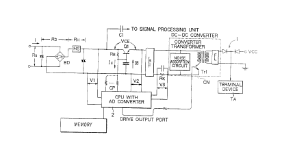
FIG. 7 is a circuit diagram of the conventional telephone line
power utility circuit 501. In this telephone line power utility
circuit 501, a direct-current voltage, which is supplied by the
telephone line through a bridge diode BD, a hook switch HS, a DC
separation transistor Ql and a low-pass filter LPF, iS converted by
a DC-DC converter CN and used as a power source for a line terminal
device main-body circuit TA. Symbol Vcc stands for a battery or the
other external power supplies to be a power source of the line
terminal device main-body circuit TA when the output from the DC-DC
converter CN is insufficient .
A signal component is processed by being taken into a signal
processing circuit (not shown in the figure) of the line terminal
equipmentmain--bodYcircuitTAthroughadirect--current interrupting
capacitor Cl behind the hook switch HS.
A drive output circuit DO pul~e-drives a switching element Trl of
the DC--DC converter CN at a predetermined duty ratio.
- la - 2 o 9 7 4 4 9
FIG. 8 is a schematic diagram of a direct-current circuit formed of an
exchange plant, telephone lines, and line terminal device. A direct-current resistance RS
B
2097449
of the line terminal equipment viewed from the telephone line-side is the sum of the
direct-current resistance RD of the bridge diode BD, a direct-current resistance RH of the
hook switch HS and an input direct-current resistance RI of the DC-DC converter,
satisfying the following equation,
RS = RD + RH + RI (1).
The direct-current resistance RS, in accordance with the JATE (Japanese
Approval Institute for Teleconllllullication Equipment) standards, for example, is regulated
at 50Q to 300Q when the line current I is 20 mA to 120 mA. The direct-current resistance
RS, in accordance with the FCC (Federal Communications Commission, USA) standards,
for example, is regulated below 200 when the line current 1 is 30 mA to 120 mA. The
line current I satisfies,
I = E / (Rl + R2 + RS) (2),
where, E represents a direct-current output voltage of the exchange plant, Rl a
direct-current resistance of the exchange plant, and R2 a line resistance. The sum Rl +
R2, fluctuates depending on a length of the line, but normally is greater than RS.
When the input direct-current resistance RI of the DC-DC converter is large,
the DC-DC converter CN receives the direct-current power from the telephone line-side
with a high efficiency.
However, the problem encountered in the conventional telephone line power
utility circuit 501 is that, the receiving efficiency is low since the input direct-current
~,g
209744~
resistance RI of the DC-DC converter CN is fixed at a lower value as a whole such that
the direct-current resistance RS of the line terminal equipment viewed from the telephone
line-side, takes a resistance value between 50Q and 300Q.
SUMMARY OF THE INVENTION
5It is a general object of this invention to provide a telephone line power
utility circuit capable of improving the receiving efficiency.
In the first embodiment, a telephone line power utility circuit of this
invention, in which a direct-current power supplied from a telephone line-side is utilized
as a power source for a line terminal equipment includes a DC-DC converter connected
10with the line terminal equipment, for supplying the direct-current power to the line
terminal equipment, and; an input direct-current resistance control means for controlling
an input direct-current resistance of the DC-DC converter for increasing a receiving power
of the DC-DC converter and for allowing a direct-current resistance of the line terminal
equipment viewed from the telephone line-side to be within a predetermined range.
15In the above mentioned first characteristic of this telephone line power utility
circuit, the input direct-current resistance of the DC-DC converter is controlled in such
a way that, the input direct-current resistance RI of the DC-DC converter is made larger
within a range, where the direct-current resistance of the line terminal equipment, viewed
from the telephone line-side, is within the predetermined range even if the line current
varies.
In a second embodiment, a telephone line power utility circuit of this
invention, in which a direct-current power supplied from a telephone line-side is utilized
as a power source for a line terminal equipment includes a DC-DC converter cormected
~4~ 20974~9
with the line terminal equipment, for supplying the direct-current power to the line
terminal equipment and for supplying the direct-current power to the line terminal
equipment, and a duty ratio control means for controlling a duty ratio of a primary side
switching element of the DC-DC converter for increasing the receiving power of the
DC-DC converter and for allowing a direct-current resistance of the line terminal
equipment viewed from the telephone line-side to be within a predetermined range.
In the above mentioned second characteristic of this telephone line power
utility circuit, the duty ratio of the primary side switching element of the DC-DC
converter is controlled in such a way that, the input direct-current resistance RI of the
DC-DC converter is made larger within a range, where the direct-current resistance
of the line terminal equipment, viewed from the telephone line-side, is within the
predetermined range even if the line current varies.
In a third embodiment, the telephone line power utility circuit of this
invention, in which a direct-current power supplied from a telephone line-side is utilized
as a power source for a line terminal equipment includes a DC-DC converter connected
with the line terminal equipment, for supplying the direct-current power to the line
terminal equipment, and a transformer tap changer means for switching taps of a primary
side winding of a transformer of the DC-DC converter for increasing the receiving power
of the DC-DC converter and for allowing a direct-current resistance of the line terminal
equipment viewed from the telephone line-side is within a predetermined range.
In the above mentioned third characteristic of this telephone line power utilitycircuit, the input direct-current resistance is controlled by switching the taps of the
primary side winding of the transformer of the DC-DC converter in such a way that, the
input direct-current resistance RI of the DC-DC converter is made larger within a range,
,.
~!B
~,.
- 5 -
2097449
where the direct-current resistance of the line terminal equipment, viewed from the
telephone line-side, is within the predetermined range even if the line current varies.
Due to the above mentioned three characteristics of the present invention, a
direct-current power supplied from the telephone line can effectively be received.
5BRIEF DESCRIPTION OF THE DRAWINGS
The present invention is illustrated diagrammatically in the following
drawings, wherein:
FIG. 1 is a circuit diagram of a telephone line power utility circuit in
accordance with a first embodiment of this invention.
10 FIG. 2 is a flow chart showing operation of the telephone line power utility
circuit shown in FIG. 1.
FIG. 3 is a circuit diagram of a telephone line power utility circuit in
accordance with a second embodiment of this invention.
FIG. 4 is a flow chart showing operation of the telephone line power utility
15circuit shown in FIG. 3,
FIG. 5 is a circuit diagram of a telephone line power utility circuit in
accordance with a third embodiment of this invention.
FIG. 6 is a flow chart showing operation of the telephone line power utility
circuit shown in FIG. 5.
20 FIG. 7 is a circuit diagram of the conventional telephone line power utility
circuit; and
FIG. 8 is a schematic diagram of a direct-current circuit.
, ~
~ ..
- 6 -
209744~
DESCRIPTION OF THE PREFERRED EMBODIMENT
The embodiments of this invention will be described in more detail with
reference to the accompanying drawings. While the embodiments of the present invention,
as herein disclosed, constitute a preferred form, it is to be understood that other forms
might be adopted.
FIRST EMBODIMENT
Fig. 1 is a circuit diagram of a telephone line power utility circuit 1
according to a first embodiment of this invention. In the telephone line power utility
circuit 1, a direct-current voltage, which is supplied from the telephone line-side through
a bridge diode BD, a hook switch HS, a DC separation transistor Q1, and a low-pass filter
LPF, is converted by a DC-DC converter CN, and used as a power source for a lineterrninal device main-body circuit TA. Symbol Vcc stands for a battery or any other
external power supplied to a power source for the line terminal device main-body circuit
TA when the output from the DC-DC converter CN is insufficient.
A signal component is processed by being taken in a signal processing circuit
(not shown in the diagram) of the line terminal device main-body circuit TA through a
direct-current interrupting capacitor C1 behind the hook switch HS.
A CPU (marked 2 in the diagram) having an AD converter, pulse-drives a
switching element Trl of the DC-DC converter CN and controls its duty ratio for
obtaining a maximum value of an input direct-current resistance RI of the DC-DC
converter CN within a range equal to or less than 300Q of a direct-current resistance of
a line terminal equipment viewed from the telephone line-side. This CPU also controls the
bias voltage such as to prevent a voltage drop in the DC separation transistor Q1 from
being equal to or more than a required proper value.
~B
~ . t
~7~ 20q7449
Thereby, loss in the DC separation transistor Ql is minimi~ed,
and the direct-current power supplied through the telephone line can be effectively
received.
FIG. 2 is a flow chart showing operations of the CPU 2 having the AD
converter. When the hook switch HS is in an off hook state (step STl), a voltage V3 in
FIG. 1 is detected (step ST2) and line current I is calculated in the next step (step ST3)
according to the equation,
I = V3 / Rk.
where, Rk represents a resistance value of a current detecting resistance.
Next, it is determined whether or not the line current I reaches a mini,llul"
current (approximately 15 mA) of the telephone line (step ST4). If the line current I does
not reach the Illinillllllll current, a control proceeds to step ST5, and if it reaches the
minimum current, the control proceeds to step ST6.
In step ST5, the DC-DC converter CN is switched off and the control returns
to step ST2.
In step ST6, the DC-DC converter CN is switched on. Here, the duty ratio,
which pulse-drives the switching element Trl of the DC-DC converter CN, is in the
memory. If no duty ratio is stored in the memory, a maximum duty ratio within a range
to be controllable (then, the input direct-current resistance RI of the DC-DC converter CN
becomes a mil~illllllll value) is assumed. The maximum duty ratio within a range to be
controllable means the m~ximllm duty ratio at which the DC-DC converter functions
properly.
B
~ .
- 8 - 2097449
The CPU 2 having the AD converter detects the voltages Vl and V2 in FIG.
1 (step ST7), and calculates the voltage VCE of the DC separation transistor Ql (the
voltage across the collector and the emitter) (step ST8).
The voltage VCE is compared with a proper value (step ST9). This proper
value is, for example, an extent of 1/2 the amplitude (2 V in case of modem) of the signal
component.
If the voltage VCE is greater than the proper value, then the control proceeds
to step ST10. If the voltage VCE is less than proper value, then the control proceeds to
step STl 1. If the voltage VCE equals the proper value, then the control proceeds to step
ST12.
In step ST10, the control port CP is controlled to enlarge the bias shunt
resistance value and to decrease the bias control current Iu. Thus, the bias current IB
becomes large and the collector-emitter voltage VCE tends to be smaller.
In step STll, the control port CP is controlled to decrease the bias shunt
resistance value and to increase the bias control current Iu. Due to this, the bias current
lB becomes small and the collector-emitter voltage VCE tends to be higher.
Finally, the voltage VCE is made to converge to the proper value through
the operations from step ST7 to step STll.
In the step ST12, the voltages Vl and V3 are detected.
Next, a direct-current resistance RS of the telephone line power utility circuit1 as viewed from the telephone line-side is calculated (step ST13) using,
I = V3 / Rk and
RS = (Vl/I) + (RD + RH).
-9- 2097449
Next, the direct-current resistance RS is compared with 300Q (preferably,
compared with the value a little smaller than 300~2) (step ST14). If RS is greater than
300Q, then the control proceeds to step ST15. If RS is less than 300Q, then the control
proceeds to step ST16. If RS equals to 300Q, then the control returns to step ST2
described.
In step ST15, the duty ratio of a drive output from the drive output port is
increased from the present value. Due to this, the direct-current resistance RS decreases.
Thereafter, the said duty ratio is stored in the memory, and then the control returns to
step ST2.
In step ST16, the duty ratio of the drive output from the drive output port
is decreased from its present value. Due to this, the direct-current resistance RS
increases. Thereafter, the said duty ratio is stored in the memory, and then the control
returns to step ST2.
In this way, the direct-current resistance RS is converged into 300 --- by
operations from step ST12 to step ST16.
SECOND EMBODIMENT
FIG. 3 is a circuit diagram of a telephone line power utility circuit 101
according to a second embodiment of the present invention. The construction of the
telephone line power utility circuit 101 is substantially the same as the telephone line
power utility circuit 1 shown in FIG. 1. The difference in the two is that a plurality of
taps are provided on a primary side of a converter transformer of a DC-DC converter CN'
and connected with switching elements Trl to Trn respectively, which are selected and
operated alternatively by the CPU (marked 22 in the diagram) having an AD converter.
~ :J ~f:
- - lO- 2097449
By selecting the switching elements alternatively from Trl to Trn, the taps
at the primary side of the converter transformer are switched and controlled for obtaining
the m~ximnm value of an input direct-current resistance RI of the DC-DC converter CN'
within a range equal to or less than 300Q of the direct-current resistance of the line
terminal device viewed from the telephone line-side. This provides an effective receiving
of the direct-current power supplied from the telephone line.
FIG. 4 is a flow chart showing operations of the CPU 22 having the AD
converter. The flow chart in FIG. 4 is very much similar to the already described flow
chart of FIG. 2 with the differences that, ST6 in FIG. 2 is changed to SU6, and steps
ST15, ST16 in FIG. 2 are changed to SU15, SU16 respectively. Accordingly, only steps
SU6, SU15, and SU16 will be described below.
In step SU6, the DC-DC converter CN' is switched on. Then, the number
of switching elements for alternatively operating are stored in the memory along with the
number of windings of the different switching elements. When information regarding the
switching element is not stored in the memory, then a switching element with theminimllm number of turns of the winding (then, the input direct-current resistance RI of
the DC-DC converter CN' becomes a minimllm value)is considered.
In step SU15, the switching element with the number of turns of the winding
less than the present number of turns, is selected. Thus, the direct-current re~i~t~nre RS
decreases. Thereafter, this switching element is stored in the memory, and then the
control returns to step ST2.
In step SU16, the switching element with the number of turns of the winding
greater than the present number of turns, is selected. Thus, the direct-current resistance
RS increases. Thereafter, this switching element is stored in the memory, and then the
.
......
11- 2097449
control returns to step ST2.
Consequently, the direct-current power supplied from the
telephone line is effectively received.
THIRD EMBODIMENT
FIG. 5 is a circuit diagram of a telephone line power utility circuit 201
according to a third embodiment of the present invention. In the telephone line power
utility circuit 201, a direct-current voltage, which is supplied from the telephone line-side
through a bridge diode BD, a hook switch HS, a DC separation transistor Ql, and
a low-pass filter LPF, is converted by a DC-DC converter CN and used as a power source
for a line terminal device main-body circuit TA. Symbol Vcc stands for a battery or any
other external power supplies to be a power source for the line terminal device main-body
circuit TA when the output from the DC-DC converter CN is insufficient.
A signal component is processed by being taken in a signal processing circuit
(not shown in the diagMm) of the line terminal device main-body circuit TA through a
direct-current interrupting capacitor Cl behind the hook switch HS.
A CPU (marked 32 in the diagram) having an AD converter, pulse-drives
a primary side switching element Tra of the DC-DC converter CN and controls a duty
ratio for obtaining the maximum value of an input direct-current resistance RI of the
DC-DC converter CN within a range equal to or less than 300Q of the direct-current
resistance of the line terminal equipment viewed from the telephone line-side. This CPU
also controls the bias voltage in order to prevent a voltage drop in the DC separation
transistor Q1 from being equal to or more than a required proper value.
This provides an effective receiving of the direct-current power supplied from
.
.~,
, . ,, ....- ~
- - 12- 2097449
the telephone line.
FIG. 6 is a flow chart showing operations of the CPU 32 having the AD
converter. A hook switch HS is placed in an OFF hook state (step SVl), then the voltage
V3 in FIG. 5 is cletectecl (step SV2), and line current I is calculated (step SV3) using,
I = V3/Rk,
where, Rk represents a resistance value of a current detecting resistance.
Next, it is determined whether or not the line current I reaches a mi"i",~
current (approximately 15 mA). If the line current I does not reach the milli,,,ll,,, current,
then the control proceeds to step SV5, and if it reaches the ~ini",u,l, current, then the
control proceeds to step SV6.
In step SV5, the DC-DC converter CN is switched off and the control returns
to step SV2.
In step SV6, the DC-DC converter CN is switched on. Here, the duty ratio,
which pulse-drives a primary side switching element Tra of the DC-DC converter CN is
stored in the memory. If no duty ratio is stored in the memory then, a m~xim~lm duty
ratio within a range to be controllable (then, the input direct-current resistance RI of the
DC-DC converter CN becomes a minimllm value) is assumed.
Next, the CPU 32 having the AD converter detects voltages Vl and V2 in
FIG. 5 (step SV7), and calculates a voltage VCE (a voltage across a collector and an
emitter) of the DC separation transistor Ql (step SV8).
The voltage VCE is compared with a proper value (step SV9). This proper
value is, for example, approximately 1/2 the amplitude (2 V in case of modem) of signal
'B '
~.
- - -
- 13 -
209744q
component.
If voltage VCE is greater than the proper value, then the control proceeds
to step SV10. If voltage VCE is less than the proper value, then the control proceeds to
step SV11. If the voltage VCE is equal to the proper value, then the control proceeds to
step SV12.
In step SV10, the control port CP is controlled to enlarge the bias shunt
resistance value and to decrease the bias control current Iu. Due to this, the bias current
IB increases and the collector-emitter voltage VCE tends to be smaller.
In step SV11, the control port CP is controlled to decrease the bias shunt
resistance value and to increase the bias control current Iu. Due to this, the bias current
IB becomes small and the collector-emitter voltage VCE is varied to be higher.
Finally, the voltage VCE is made to converge to the proper value through
the operations from step SV7 to step SV11.
In step SV12, the voltages V1 and V3 are detected.
Next, a direct-current resistance RS of the telephone line power utility circuit201 as viewed from the telephone line-side is calculated (step SV13) using,
I = V3 / Rk and
RS = (V1/I) + (RD + RH).
Next, the direct-current resistance RS is compared with 300Q (preferably
compared with the value a little smaller than 300Q) (step SV14). If RS is greater than
300Q, then the control proceeds to step SV15. If RS is less than 300Q, then the control
proceeds to step SV16. If RS is equal to 300Q, then the control returns to step SV2
,
_ - 14- 2097449
described earlier.
In step SV15, a duty ratio of a drive output from a drive output port is
increased from the present value. Thus, the direct-current resistance RS is smaller.
Thereafter, said duty ratio is stored in a memory, and then the control returns to step
5 SV2.
In step SV16, the duty ratio of the drive output from the drive output port
is made smaller. Thus, the direct-current resistance RS tends to be larger. Thereafter,
the duty ratio is stored in the memory, and then the control returns to step SV2.
Finally, the direct-current resistance RS is converged into 300 --- by
10 processes from step SV12 to step SV16.
As a result, the loss in the DC separation transistor Ql is minimi7~d and the
direct-current power supplied from the telephone lines is effectively received.
,. . . .