Note : Les descriptions sont présentées dans la langue officielle dans laquelle elles ont été soumises.
2 ~ 7 2
MICRO-VALVE AND METHOD OF M~NUFACTURING
The present application is concerned with
micro-valves having a movable spool and seat comprised
of silicious material.
Silicious valves are fairly well known, and
numerous publications exist dealing with their
structure and various manufacturing techniques. For
example, U.S. Patent No. 5,082,242 teaches an
electronic micro-valve which has an integral structure
made on one piece of silicon and is a flow through
valve with an inlet and an outlet on opposite sides of
the silicon wafer. The aperture for flow through the
silicon wafer is opened and closed by a movable
closure member that merely covers the aperture for
flow.
In the article "Electrically Activated,
Normally Closed Diaphragm Valves" by H. Jerman
(9lCH2817-5/91 IEEE), there is a disclosure as to
electrically activated, normally closed diaphragm
valves that have been fabricated using heated
bimetallic diaphragms to provide the operating force.
Figure 1 in the document discloses a boss which
completely covers the valve seat, thereby preventing
flow to the outlet.
In the article entitled "Smallest Dead Volume
Mlcrovalves For Integrated Chemical Analyzing Systems"
by S. Shoji, B. Van der Schoot, N. de Rooij and M.
Esashi (9lCH2817-5/91 IEEE), there is a discussion with
respect to normally open and normally closed
microvalves and a three-way microvalve. The drawings
depict a ridge in a silicious substrate which contacts
a polymer membrane, thereby controlling flow through
the inlet and outlet.
.~
2 ~ 57~
-
Numerous other references pertain to micro
machine valves and are listed as follows. U.S. Patent
Nos. 4,581,624; 4,647,013; 4,657,621; 4,670,092;
4,756,508; 4,768,751; 4,826,131; 4,869,282; 4,966,646;
5,029,805; 5,065,978; 5,082,242; and the article
entitled "Variable-Flow Micro-Valve Structure
Fabricated With Silicon Fusion Bonding" by F.
Pourahmadi, L. Christel, K. Peterson, J. Mallon and J.
Bryzek (CH2783-9/90 IEEE).
The present invention is directed towards the
provision of silicious micro-valves which have a
movable spool and/or valve seat which permits a
complete alignment with the 111 planes of the spool and
the conforming seat.
The present invention further is directed to
obtaining a conformed spool and valve seat which (i)
permits sharp edge orifice controls to thereby obtain
improved flow viscosity effects and (ii) has improved
sensitivity of the valve and thereby improved valve
performance.
In one aspect, the present invention provides
a micro-valve comprised of a movable spool and/or seat
comprising a silicious spool having three planes, and,
aligned with all of the spool's planes, a silicious
seat conforming to the spool's planes, wherein the
spool and/or the seat may move to open or close the
valve. The spool planes may be 111 planes.
In accordance with a further aspect of the
invention, there is provided a method of manufacturing
a silicious micro-valve comprising the steps of:
a. providing a first silicious substrate,
b. removing a portion of the first
substrate to reveal three planes of the substrate, the
three planes forming the valve seat,
c. growing a second substrate to conform to
the three planes of the first substrate, and
5 7 ~
d. assembling the two substrates formed
using steps (a) through (c) to form a micro-valve. The
planes of the first substrate produced are 111 planes.
In the description which follows, reference
S is made to the accompanying drawings, in which:
Figures 1 to 23 are cross-sectional views of
a silicious substrate with different materials applied
and removed in the preparation of a portion of a
microvalve;
Figure 24 is a cross-section of an assembled
open microvalvei and
Figure 25 is a cross-section of an assembled
closed microvalve.
The present invention is concerned with a
silicious microvalve and the manufacture of same. In
the drawings, a silicious substrate 10 has a silicious
nitride or oxide coating 12 applied to the substrate.
Prior to the wafer having applied the silicious nitride
thereto, the silicious wafer is treated with five parts
of sulfuric acid with one part of peroxide and is
heated at 100~C. This is a cleaning technique
2102572
FMC 0379 PUS -4-
91-528
and is generally considered a pre-treatment prior to
the application of the silicon nitride. The thickness
generally ranges from about 500 to 1000 angstroms
using commercially available ter-hniques. In general,
this is a low pressure chemical vapor deposition
(LPCVD). The reaction conditions generally are 800 C
at 300 millitorr. Reagents are generally
dichlorosilane and ammonia. Thereafter, a photoresist
16 is applied to the layer 12 using standard
integrated circuit photolithography techniques. A
typical technique is to spin coat Shipley product 1470
positive photoresist onto the silicious substrate.
The conditions are about 5000 rpm with a coating
thickness of 1.2 microns (see Fig. 2). The resist is
patterned by exposing selected regions to W light
using commercially available equipment (chrome masks
and mask aligners). After exposing the resist to W
light it is developed in a commercially available
developer, such as Hoechst Celanese MF 312. The
developer removes the resist that was exposed to W
light. The cross-section is shown in Figure 3. Next
the oxide/nitride layer is etched using the patterned
resist as a mask. First the silicon nitride is
etched, typically in a plasma etch system. A
commercially available etcher, such as a Tegal 903e
(Tegal, Inc. of Arizona), would use SF6at about 300
mTorr with a 100 watt RF field applied to form a
plasma. The sulfur hexafluoride plasma etches silicon
nitride. Once the nitride is etched the silicon
dioxide can be removed either using a plasma, or a wet
etch in a dilute HF solution. Commercially available
oxide etches will typically contain ammonium fluoride
as a buffering agent. Figure 4 shows a cross-section
2102572
FMC 0379 PUS -5-
91-528
of the structure after the oxide and nitride have been
etched, exposing silicious surface 17.
The photoresist can now be removed from the
wafer. An oxygen plasma can be used. Commercially
available systems include Branson International Plasma
Corp. of California and Technics Plasma GmbH of
Muenchen, Germany, or a wet strip of five parts of
sulfuric acid with one part of hydrogen peroxide and
heated to lOO C. Figure 5 shows the cross-section
after resist removal.
The next step is to etch the material of
Figure 5 to obtain that shown in Figure 6 with an
anisotropic etchant such as potassium hydroxide or EDP
(ethylene diamine and pyrocatechol in the presence of
water).
The etching that takes place as is shown in
Figure 6 is to a depth of about 5 to 30 microns so
that the unetched portion identified as 18 has a
silicon nitride or oxide layer. After the anisotropic
etching is complete the oxide/nitride layer is removed
from the wafer. This is done by immersing the wafer
in a 1:1 mix of HF and deionized water (DI). The
structure is shown in-cross-section in Figure 7
showing silicious surfaces 19, 21, 23 and 25.
In the next step, Figure 8, there is the
application of additional silicon oxide 20 which is
grown over the entire wafer surface. Silicon nitride
22 is then applied on top of silicon oxide. The
silicon nitride is deposited by LPCVD.
The next step as is shown in Figure 9 is the
application of a photoresist shown as reference
numeral 30. The resist is patterned using photo masks
and W light as described earlier. After developing
the resist the cross-section will look like Figure 10.
2102572
FMC 0379 PUS -6-
91-528
After the developing of the resist, the
nitride material will be etched utilizing a plasma
etching system as described earlier.
Thereafter, the resist is cleaned off. The
wafer is shown in Figure 11 uncovering surface 23. The
wafer is now placed into a diffusion furnace
(commercial manufacturers include ASM International of
Phoenix, AZ; and BTU Engineering Corp., Bruce Systems
Division of N. Billerica, MA) and heated to about
1000 C in the presence of oxygen and steam. The
oxygen and steam cause the silicon not covered with
silicon nitride to convert to silicon dioxide. The
conversion, or growth, of oxide slows down as the
thickness of the oxide increases. Figure 12 shows the
cross-section after one or two micrometers of oxide 32
have been grown. (This te~-hnique of selectively
growing oxide using a layer of silicon nitride as a
mask is commonly referred to as LOCOS, or LOCal
Oxidation of Silicon).
The nitride material is then removed such as
by hot phosphoric acid. As shown in Figure 13,
photoresist 34 is applied to the wafer and patterned.
The oxide 20 at the bottom of the pit is then etched
away using a plasma or a wet etch as described
earlier. Figure 14 shows the device cross-section
after oxide etch revealing surface 21. Note: the
sidewall oxide will also etch, but since it is so much
thicker than the oxide on the bottom of the pit any
loss in thickness is negligible. The resist is then
cleaned off of the wafer, resulting in a device cross-
section as shown in Figure 15.
Thereafter, the substrate is cleaned and
is subjected to an epi reactor, that is, epitaxial
growth occurs by depositing a silicon layer onto the
- 2102~72
FMC 0379 PUS -7-
91-528
silicon exposed at the bottom of the etch pit. This
is applied by CVD (Chemical Vapor Deposition) such as
1100 Centigrade and atmospheric pressure in the
presence of dichlorosilane and hydrogen.
Additionally, one may use diborane, phosphine or
arsine to control the conductivity of the layer. The
silicon layer is identified by reference numeral 40.
The layer takes on the characteristics of the layer
below. The layers are virtually indistinguishable
except for the electrical properties of the respective
layers (see Figure 16).
Thereafter, as is shown in Figure 17, the
wafer is ground and polished and sized to the extent
shown in Figure 17 where the layer 40 has been reduced
to surface 42. Silicon nitride 44 is applied to the
wafer. Photoresist is applied to the wafer backside
as is shown in Figure 18. The resist is patterned as
described before resulting in the cross-section shown
in Figure 19 revealing nitride layer 44. The resist
pattern is aligned to the machined regions of the
wafer by use of a two side aligner. One manufacturer
of two side aligners is Karl Suss America of Waterbury
Center, VT. The objeat is to align openings l9a and
lsb with machined segments 32 and 42. The nitride on
the backside is then etched as described earlier
resulting in the cross-section shown in Figure 20.
The resist is then stripped from the wafer as shown in
Figure 21. The silicon is then etched in one of the
anisotropic etchants mentioned earlier until the oxide
32 formed on the sidewalls described earlier is
revealed, as shown in cross-section in Figure 22. The
nitride is now stripped from the wafer giving the
cross-section shown in Figure 23, revealing surfaces
19, 25 and 42.
8 2 ~ 7 2
Two sections resulting from the process
described above, namely that shown in Figure 23, are
assembled together as shown in Figure 24. The
materials are assembled by fusion bonding. A typical
fusion bonding cycle consists of cleaning the wafers in
5:1 H2SO4:H2O2, rinsing thoroughly in deionized water,
drying in heated nitrogen, aligning and pressing the
wafers together, then heat them to approximately 1000~
Centigrade for 12 hours. The spools are released from
the valve seats by immersing in an etching mix of
hydrofluoric acid and water, which dissolves the oxide
32 grown on the etch pit sidewalls.
Figure 24 shows the two layers which permit
fluid in a final assembly having valve fluid inlet at
50. The inlet 50 is formed during previous processing
steps of etching, application of photoresist, and the
like in known fashion, even though it has not been
shown in the drawings. Fluid outlet at 52 and 52' are
formed by dissolution of oxide 32, revealing surface
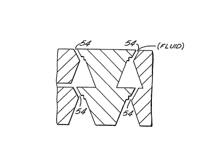
23. The closed valve is shown in Figure 25. Due to
the size of the microvalve, fluid 54 may be presenti
but there is no flow because of the construction of the
valve surfaces.
A preferred apparatus in which the above-
identified valve may be utilized is described in U.S.
Application No. 765,613, filed September 25, 1991,
entitled "Integral Antilock Brake/Traction Control
System" (Ford Motor Co. Invention Disclosure No. 92-
202).
That apparatus provides an electro-hydro-
mechanical integrated anti-lock brake and traction
control assembly wherein a linear motor acts on a
pressure control valve to provide brake pressure
O. ~
. ~ ~ia 1
'~ 2102S72
FMC 0379 PUS -9-
91-528
proportional to the voltage signal supplied to the
motor. The mode of operation, either anti-lock brake
system control or traction control, is selected by
simply changing the polarity on the linear motor.
In accordance with one aspect of that
apparatus, an integral anti-lock brake and traction
control system for a vehicle is provided which
includes a pressure control valve including a first
pressure feedback valve associated with a braking
control system and a second pressure feedback valve
associated with a traction control system. In a first
mode, means responsive to a control voltage, such as a
liner motor, are provided which activate the first
pressure feedback valve to regulate brake pressure in
the braking control system proportionally to the
control voltage which is supplied. In a second mode,
the means responsive to the control voltage activate
the second pressure feedback valve to control vehicle
traction in the traction control system. The modes
are selected by simply changing the polarity of the
control voltage signal. The valve of this invention
is the pressure feedback valve of the invention
entitled "Integral Anti-Lock Brake/Traction Control
System" described above.
While the forms of the invention herein
disclosed constitute presently preferred embodiments,
many others are possible. It is not intended herein
to mention all of the possible equivalent forms or
ramifications of the invention. It is understood that
the terms used herein are merely descriptive rather
than limiting, and that various changes may be made
without departing from the spirit or scope of the
invention.
- ~ 2102572
FMC 0379 PUS -10-
91-528
For example, an alternative to the formation
of silicon layer 40, one can dope it with boron and/or
germanium such as adding diborane and/or germane gas
and incorporate it/them into the solid. The advantage
is in its/their removal as in Figure 23; there is more
precise control to obtaining the substrate.