Note : Les descriptions sont présentées dans la langue officielle dans laquelle elles ont été soumises.
2 ~ 3 5
THE APPARATUS FOR ADJUSTING THE EFFICIENCY
OF ELECTRIC POWER AMPLIFICATION
FIELD OF THE INVENTION
This invention relates to an apparatus for
adjusting the efficiency of RF power amplification, and
more particularly to an adjusting apparatus of the RF
power amplifying efficiency in which the power
consumption of a mobile station is minim;zed in a TDMA
(time division multiple access) radio communication
system.
BACKGROUND OF THE INVENTION
A conventional apparatus for adjusting the
efficiency of power amplification is used in a portable
telephone set such as Cellular type telephone set in
which transmission and receipt of signals are carried
out simultaneously.
In the conventional adjusting apparatus of
the power amplification efficiency, an electric power
is supplied via a control circuit to a power
amplification circuit, and the control circuit detects
the electric power to be supplied to the power
amplification circuit, so that the electric power is
minimized dependent on an efficiency control signal
2~0~7~:j
supplied from the control circuit to the power
amplification circuit, provided that an output signal
of the power amplification circuit is controlled to be
constant by the control circuit. This is defined as
"efficiency control", and the efficiency control is
constantly carried out at the time of transmission.
In the conventional adjusting apparatus of
the power amplification efficiency, however, there is a
disadvantage in that an optimum efficiency is difficult
to be obtained in the case where transmission is
carried out instantly in a burst mode. Further,
there is a disadvantage in that noise is generated on a
transmission output signal, and the transmission output
signal is ~1uctuated, when a power amplification factor
is adjusted during s~nal transmission.
SUMMARY OE THE INVENTION
Accordingly, it is an object of the invention
to provide an apparatus for adjusting the efficiency of
power amplification in which the power amplification is
carried out by an optimum efficiency, even in the case
where signals are transmitted in a burst mode.
It is a further object of the invention to
provide an apparatus for adjusting the efficiency of
power amplification in which noise carried on a
transmission signal is reduced, and no fluctuation
occurs in an output signal, even if an amplification
7 3 ~
-- 3
factor is adjusted in an power amplification circuit during
the signal transmission.
According to one aspect of the invention, there is
provided an apparatus for adjusting the efficiency of power
amplification, comprising: a power amplification circuit for
amplifying a signal to be transmitted in a time division
multiple access mode; and a control circuit for controlling
the efficiency of power amplification in said power
amplification circuit comprising a circuit for detecting an
electric current supplied from a power supply to said power
amplification circuit; wherein said efficiency is controlled
in said control circuit by one of a sum and a difference of
values of said electric current detected at two adjacent
transmission periods, said efficiency being controlled to be
an optimum value at a period not belonging to a period for
said signal to be transmitted.
According to another aspect, the present invention
provides an apparatus for controlling an efficiency control
signal to be supplied to a power amplification circuit in a
time division multiple access mode, comprising: means for
detecting an electric power supplied from a power supply to
said power amplification circuit at a present signal
transmitting period; means for detecting whether said electric
power is increased or decreased at a period between a signal
transmitting period preceding to said present signal
transmitting period and said present signal transmitting
period, thereby generating an increased signal, when said
,~
71885-32
7 3 ~
- 3a -
electric power is increased, and a decrease signal, when said
electric power is decreased, respectively; means for
generating said efficiency control signal which is dependent
on said increase and decrease signals, said efficiency control
signal being a value obtained by subtracting a control value
from an efficiency control signal used at said signal
transmitting period preceding to said present signal
transmitting period, when said increase signal is generated,
and said efficiency control signal being a value obtained by
adding said control value to said efficiency control signal
used at said signal transmitting period preceding to said
present signal transmitting period, when said decrease signal
is generated.
BRIEF DESCRIPTION OF THE DRAWINGS
The invention will be explained in more detail in
conjunction with appended drawings, wherein:
Fig. 1 is a block diagram showing a mobile station,
Fig. 2 is a block diagram showing a conventional
apparatus for adjusting the efficiency of power amplification
included in the mobile station,
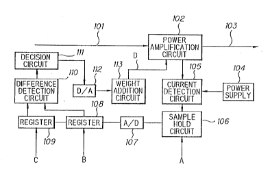
Fig. 3 is a block diagram showing an apparatus for
adjusting the efficiency of power amplification in a first
preferred embodiment according to the invention,
71885-32
-- 2~ 02~
Fig. 4A is a timing chart explaining
operation in the first preferred embodiment, and
Fig. 4B is a graph explaining the relation
between the efficiency control value and the
efficiency.
DETAILED DESCRIPTION OF THE PREFERRED EMBODIMENTS
Fig. 1 shows a mobile station including a
conventional apparatus for adjusting the efficiency of
power amplification. The mobile station comprises
a baseband signal processing circuit 211 for generating
a baseband signal, a modulation circuit 210 for
modulating the baseband signal by a signal to be
transmitted, a power amplification circuit 202 for
amplifying the modulated signal, a common use circuit
214 for supplying the amplified signal to an antenna
215, from which the amplified signal is transmitted,
and for supplying a signal received by the antenna 215
to a low noise amplification circuit 213, in which the
received signal is amplified by suppressing the
generation of noise, a demodulator 212 for demodulating
the received signal supplied from the low noise
amplifier 213 to obtain a transmitted signal, and a
control circuit 205 for controlling the power
amplification circuit 202 to amplify the modulated
signal by a controlled efficiency and the baseband
signal processing circuit 211 to generate the baseband
- 2 ~
slgnal .
Fig. 2 6hows the conventional apparatus for
adjusting the efficiency of power amplification which
comprises the control circuit 205 as shown in Fig. 1, a
power supply 204 and the power amplification circuit
202 as also shown in Fig. 1.
In operation, a baseband signal is generated
in the baseband signal processing circuit 211 by
processing a received baseband signal supplied from the
demodulator 212. The baseband signal thus
generated is modulated in the modulation circuit 210 to
provide the modulated signal by a signal to be
transmitted from the antenna 215, and the modulated
signal is amplified in the power amplification circuit
202 by the control circuit 205.
In the control circuit 205, an electric power
203 supplied from the power supply 204 to the power
amplification circuit 202 is detected, and the detected
electric power 203 is controlled to be minimized by
generating an efficiency control signal 201 to be
supplied to the power amplification circuit 202.
Consequently, a power amplification efficiency is
adjusted in the power amplification circuit 202, so
that an output signal of the power amplification
circuit 202 is controlled to be constant during the
whole time of a signal transmission period.
Thus, a constant power of the modulated and amplified
- 2~0273~
signal i8 transmitted via the eommon use eireuit 214
from the antenna 215. In this explanation, a signal
reeeiving operation is omitted, because it is self-
explanatory.
However, the aforementioned disadvantages
occur in the eonventional apparatus for adjusting the
efficieney of power amplifieation.
Next, an apparatus for adjusting the
effieieney of power amplifieation in the preferred
embodiment aeeording to the invention will be explained
in Fig. 3.
The apparatus for adjusting the effieieney of
power amplifieation eomprises a power amplification
cireuit 102, a power supply 104, a eurrent deteetion
eireuit 105, a sample hold eireuit 106, an analog to
digital (A/D) eonverter 107, registers 108 and 109, a
differenee deteetion cireuit 110, a decision circuit
111, and a digital to analog cireuit 112, a weight
addition eireuit 113.
In operation (to be explained in Fig. 4A), an
input signal 101 is amplified in the power
amplifieation eireuit 102 to generate an output signal
103, wherein an electrie power is supplied via the
current detection circuit 105 from the power supply 104
to the power amplification circuit 102. A eurrent
value deteeted in the eurrent detection cireuit 105 is
supplied to the sample hold cireuit 106, in which the
2 ~ O ~ E ~; ~
current value is sampled at a rising edge of an input
clock A generated at a transmission time TX and held at
a falling edge of the input clock A. The current
value held in the sample hold circuit 106 is converted
in the A/D converter 107 from an analog value to a
digital value. A content of the register 108 is
read to be stored in the register 109 at a rising edge
of an input clock C generated prior to a receipt time
RX, and supplied threrfrom to the difference detection
circuit 110 at the same time, and the register 108
reads a content of the A/D converter 107 at a rising
edge of an input clock B generated at the receipt time
RX. In other words, the content of the A/D
converter 107 and the register 108 are transferred to
the register 108 and the register 109, respectively, at
a period prior to a subsequent transmission time TX.
Then, the contents of the registers 108 and
109 are supplied to the difference detection circuit
110, so that a difference between the contents thereof
is detected therein to be supplied to the decision
circuit 111. The decision circuit 111 has stored
an increased amount between a former output value of
the decision circuit 111 and an output value preceding
the former output value, wherein the decision circuit
111 decides whether the detected current in the current
detection circuit 105 is increased or not in accordance
with the difference supplied from the difference
- 2~27~
detection circuit 110. Here, it is assumed that
the power amplification circuit 102 has a property as
shown in Fig. 4B. Thus, when it is detected in the
decision circuit 111 that, the detected current is
increased, an output value (present control value) of
the decision circuit 111 is a value obtained by adding
a polarity-inverted value of the increased (stored)
amount to the former output value, and, when it is
detected in the decision circuit 111 that the detected
current is decreased, the output value of (present
control value) of the decision circuit 111 is a value
obtained by adding the increased (stored) amount to the
former output value. The present control value is
supplied to the D/A converter 112, in which an analog
control signal is obtained, and the analog control
signal is amplified in the weight addition circuit 113,
so that the amplified control signal is supplied as an
amplification efficiency control signal D to the power
amplification circuit 102. This control is repeated
to provide an optimum power amplification efficiency.
Although the invention has been described
with respect to specific embodiment for complete and
clear disclosure, the appended claims are not to be
thus limited but are to be construed as embodying all
modification and alternative constructions that may be
occur to one skilled in the art which fairly fall
within the basic teaching here is set forth.