Note : Les descriptions sont présentées dans la langue officielle dans laquelle elles ont été soumises.
21036~7
.. . . ..
.
VARIABL~ FR~QU~NCY ~L~CTRONIC BALLAST OF
NIGH POWER ~ACTOR AND STABILIZ~D OUTPUT VOLTAG~
: '
The present invention relates to an electronic ballast ~- -
system, and more particulary to a variable frequency electronic -
ballast system of high power-factor and stabilized output-
voltage, which is used for fluorescent lamps and other gas
discharge lamps. -
Electronic ballast systems for fluorescent lamps and other
gas discharge lamps are known in the art. However, in most of
prior art electronic ballast systems, the principle of
operation is: First, the input AC power is changed to a
constant DC voltage power by a rectifier and a filter, then a
DC/AC inverter is used to change the DC voltage power to high
frequency voltage power to light the lamp. Because the
inverter only works in the waveless DC power, the system must
use a big filter capacitor to filter off the pulsating wave
after rectifying. Therefore, the system has input current only
when the input voltage exceeds the voltage of the filter - ;
capacitor. The result is that the input current waveform is
distorted, which causes low power-factor and high quantity of
harmonics for the input AC power.
The present invention provides a substantially variable
freguency electronic ballast system having an AC power source
for actuating at least one gas discharge lamp. The ballast
system comprising: A rectifying circuit is connected to the AC
power source for supplying a full-wave rectified pulsating DC
voltage. A voltage-controlled oscillator is connected to the
pulsating DC voltage ~or establishing a substantially high
frequency oscillating signal, the frequency of this signal
varies with the pulsating DC voltage. A driving circuit is
connected to the oscillator for amplifying the high freguency
oscillating signal. An electronic switch is connected to the
driving circuit, the pulsating DC voltage is coupled to the
electronic switch as a power supply, for providing an inverted ~ :
high frequency square-wave voltage power. A resonant circuit -
is linked between the electronic switch and the lamp for
establishing a stabilized output-voltage.
Said rectifying circuit includes a full-wave rectifier.
_ . . ~ . , - ,.
. .
-- 2la3627
`~
The rectifying circuit may also have a small capacitor for
preventing the output voltage being reduced to zero, but the
capacitor must be so small that the output of the rectifying
circuit still maintains more than fifty percent original
pulsation.
Said voltage-controlled oscillator includes a linear
voltage-controlled oscillator, the function of which is that
the output frequency varies with the input voltage. The
voltage-controlled oscillator may also have a nonlinear
corrector for correcting output nonlinear difference of the
ballast system, which is caused by said resonant circuit. The
nonlinear corrector has at least one nonlinear device; for ~-
example: Zener diode etc.
Said driving circuit has at least one amplifier, the
function of which is to amplify the oscillating sigDal.
Said electronic switch has at least one semiconductor
device, for example: Transistor, SCR, MOSFET, IC etc., the
function of which is to invert the pulsating DC voltage to high
frequency voltage.
Said resonant circuit consists of at least one inductor
and at least one capacitor, the function of which is when the
operating frequency changes, the rate of input/output voltage
also changes in the resonant circuit. In the present
invention, some electronic ballast systems may be applled for
two or more lamps. In this case, the resonant circuit has the
same number of groups of output terminals, for actuating the
lamps.
Various other advantages of the present invention will be
readily apparent from the following detailed description when
considered in connection with the accompanying drawing forming
a part thereof and in which:
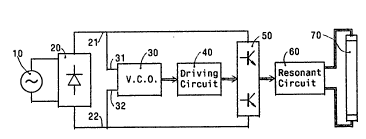
Figure 1 is a block diagram shown in said variable
frequency electronic ballast system embodying the present
invention;
Figure 2 is a practical schematic circuit of the present
invention;
Figure 3 is a practical schematic circuit of the V.C.O.
and Driving module.
Referring to the Figure 1, there is shown the block
4~ diagram of a variable frequency electronic ballast system. In
Figure 1, an AC power source 10 is applied to a rectifying
~ 21~3627
_ . .:
circuit 20, the output of rectifying circuit 20 is a full-wave
rectified pulsating DC voltage and supplied to the DC lines 21
and 22. A voltage-controlled oscillator 30 is connected to the
DC lines 21 and 22 at its input terminals 31 and 32. A driving
circuit 40 is connected between the oscillator 30 and an
electronic switch S0, for amplifying the high frequency signal
from the oscillator 30 to trigger the electronic switch 50.
The DC lines 21 and 22 are also connected to the electronic - ~:
switch 50 as a power supply; the electronic switch S0 inverts ~ -- -
the pulsating DC voltage to the high frequency voltage but the
high frequency voltage still includes the pulsating component.
A resonant circuit 60 is applied to smooth pulsation of the
high frequency voltage, which is linked between the electronic
switch 50 and the lamp 70.
The practicable circuits of the present invention may be --
designed in various ways. Figure 2 just shows one of them.
In Figure 2, an AC power source 10 of sinusoidal voltage
is applied to a rectifying circuit 20, the unidirectional
pulsating voltage output of which is supplied directly between
the DC lines 21 and 22, with the positive voltage being ~ -
connected to the line 21. The rectifying circuit 20 consists
of a full-wave bridge rectifier 23 and a small capacitor 24.
The volume of small capacitor 24 is about 1/5 to 1/10 of a ~ -
regular filter capacitor. In this system, a voltage-controlled
oscillator with a nonlinear corrector and a driving circuit are
made up of a V.C.O. and Driver module 90. For more
description, a schematic circuit of the module 90 is shown in
Figure 3. The electronic switch 50 includes two serial
transistors 51 and 52, four driving output terminals 41, 42, 43
and 44 from module 90 which are connected to the bases and the
emitters of transistors 51 and 52 respectively; the serial
connection point of transistors 51 and 52 is as an output
terminal of electronic switch 50; the collector of transistor
Sl and emitter of transistor 52 are connected to the DC lines
21 and 22 respectively. The resonant circuit 60 has two groups
of output terminals and connected to two lamps 71 and 72. In
the resonant circuit 60, the inductors 61, 64 and the
capacitors 62, 63, 65, 66 compose two similar resonant networks
respectively.
Figure 3 shows the detail of V.CØ and Driver module 90.
In the Figure 3, the module 90 has a voltage-controlled
3 ~ ~ ~
::
::
:: :
` 2103627
"' '
oscillator 30 with a nonlinear corrector, a driving circuit 40
and a simple supplying circuit. The supplying circuit includes
a diode 91, two voltage reducing resistors 92, 93 and two
filter capacitors 94, 95. The voltage-controlled oscillator
with a nonlinear corrector 30 is composed of two parts: One is
a nonlinear corrector part, which includes four resistors 33,
34, 35, 36, a zener diode 37 and a transistor 38~ Another part
is a linear voltage-controlled oscillator 39, which may consist
of an IC (for example LM3900, CD4007) and surrounding elements.
(Reference- C. Sondgeroth, More PLL Magic, 73 Magazine, Aug.
1976, p 56-59; \ W.J. Prudhomme, CMOS Oscillators, 73 Magazine,
July 1977, p 60-63). The driving circuit includes a driving
transistor 45 and a driving transformer 46.
The operation of the circuit of Figure 2 and Figure 3 may
be explained as follows:
In Figure 2, the AC power source 10 represents an ordinary
electric utility power line, the nominal value of which is
120V/60Hz, the voltage from which is applied directly to the
bridge rectifier identified as 23. This bridge rectifier is of
conventional construction and provides for the full-wave
rectified voltage to be applied to the V.C.O. and Driver module
90 and the electronic switch 50 by way of the DC lines 21 and
22. The small volume capacitor 24 is connected directly across
the output of the bridge rectifier 23, in which a little energy
is stored so that when the output voltage of the bridge
rectifier is going to be zero, the energY is discharged from
the capacitor 24 keeping the DC voltage above zero. But the
capacitor 24 is so small that the DC voltage is still
pulsating, and the valley and peak values are about 40V - 160V.
The V.C.O. and Driving module 90 is connected as Figure 2 and
inside operation of which is as Figure 3.
In Figure 3, the pulsating DC voltage is entered from
input terminals 31 and 32. A part of the current becomes DC
supply by way of the diode 91 and the resistors 92 and 93. In
this DC supply circuit, the function of diode 91 is to prevent
the current returning to terminal 31. The resistors 92 and 93
are used to reduce the DC voltage, and the capacitors 94 and 95
are used for filtering pulsation of the DC voltage. The
voltage at the capacitor 94 is applied to the oscillator 30 and
4Q the value is about 18V; the voltage at the capacitor 95 is
applied to the driving circuit 40 and the value is about 80V,
2103627
. . ~
but the values of voltage may be different than the aforesaid,
although that depends on what devices are to be used. Besides
this use, the pulsating DC voltage is divided by the resistors
33 and 34, then offered to the base of the transistor 38. The
transistor 38 and the resistor 35 compose an inverting
amplifier and a controlled voltage signal is from the collector
of transistor 38. The resistor 36 parallel with the zener
diode 37 compose a nonlinear circuit, through which the
controlled voltage signal passes into the linear voltage-
controlled oscillator 39. The output of linear voltage-
controlled oscillator 39 is a high frequency signal, the
frequency of which varies with the controlled voltage signal
and its value is about 20 KHz to 40 KHz. The high frequency
signal is provided to the base of the driving transistor 45 and
is amplified. The amplified high frequency signal is from the
collector of transistor 45, which circulates through the
primary winding of the driving transformer 46. The output of
the driving transformer is two high frequency square-wave
signals from secondary windings of driving transformer 41 and
48, which are of the same value and opposite phase. The output
terminals of the driving signal are identified as 41, 42, 43
and 44 on the module 90.
Bac~ to Figure 2, two serial transistors 51 and 52 compose
an electronic switch 50. The terminals 41, 42, 43 and 44 are
directly connected to emitters and bases of transistors 51 and
52, and the transistors 51 and 52 switch with the driving
signals by turn. A high frequency square-wave voltage power of
which frequency and voltage both vary with pulsation of
pulsating DC voltage, with output from the emitter of
transistor 51 going into the resonant circuit. The resonant
circuit has two of the same resonant networks. Each resonant
network has an inductor 61 (or 64) in series with a capacitor
62 (or 65), another capacitor 63 (or 66) in parallel with the
lamp 71 (or 72) and the lamp 71 (or 72) is in series with the
resonant network by way of its filaments. The resonant
frequency of the network is designed near and higher than the
maximal operating frequency of the electronic switch, and the
frequency - output/input characteristic is the higher the
operating frequency the greater the voltage rate of
output/input. Therefore, when DC voltage between the DC lines
21 and 22 is on the increase, the oscillating frequency of the
.
-; ,~
- ,. .
21~3~27
: :
module 90 is decreased. At output of electronic switch 50, the
result is that the voltage is increased simultaneously with the
decrease in frequency. 8ecause in the resonant circuit, the
voltage rate of output/input is decreased with reduction of the
operating frequency, when the voltage from electronic switch 50
is increased, which frequency is decreased and the output
voltage is decreased to compare with the input voltage. In
other words, the output voltage of the resonant circuit is
stabilized. The voltage rate of output/input varies with the
operating frequency that is usually not linear, and for gaining
better compensation, the nonlinear corrector is used. If the
frequency - output/input characteristic of resonant circuit is
linear enough, the nonlinear corrector would not be used. The
voltage-controlled oscillator 30 is the linear voltage-
controlled oscillator 39.