Note : Les descriptions sont présentées dans la langue officielle dans laquelle elles ont été soumises.
TITLE OF THE INVENTION
SEMICONDUCTOR VALVE
BACKGROUND OF THE INVENTION
Field of the Invention
This invention relates to a semiconductor valve in
which high-speed, high-voltage switching valve devices
(hereinbelow called "semiconductor devices") are connected
in series.
Description of the Related Art
In thyristor valves employed in D.C. power
transmission, frequency conversion or reactive power
regulation etc., the voltage rating of each thyristor is at
most 6 kv. Usually therefore a number of thyristors on the
order of several tens to one hundred are connected in
series. In this case, there is a risk of failure due to
overvoltage unless a large number of thyristors execute
identical operation. Generally, therefore, the thyristors
are selectively employed. For example, in the "Points to be
noted in connection with series connection" in Section 2.5
of "Power Electronics" by Kohji Imai, published in 19~~ by
- 1 -
Denki Shoin, it is indicated that, in order to suppress the
variation in the sharing voltages on turn-off to the
prescribed value, it is necessary to keep the variation in
the thyristor recovery charges within a certain range.
As an example for switching valve devices, in Section
5.4 of "Turn-off thyristors" by Nagataka Seki, et al.,
published in 1983 by Denki Shoin, it is indicated, in order
to suppress the variation in sharing voltages on turn-off of
series-connected GTOs to the prescribed value, it is
necessary to control the variation in the storage times of
GTOs.
Fig. 3 is a view given in explanation of the waveforms
of the anode current I, the gate current Ig and the anode
voltage V, on GTO turn-off. Taking the variation in the
storage times of two GTOs as Ots, the cut-off current as I,
and the variation in the electric charges as ~Q1 when two
GTOs are connected in series, these may be expressed
approximately by the following equation.
OQ1 = pts.I
pQ1 is equal to the variation in the electric charges
of the snubber capacitors, so if the variation in the
sharing voltages is subsequently taken to be OV, then,
taking the capacitance of the snubber capacitor as C, we
have:
- 2 -
21~'~~3~
~V = OQ1/C = ~ts.I/C ....................................
In a GTO, current turn-off is effected by shifting
current to a snubber capacitor. The capacitance of the
snubber capacitor is therefore closely linked to the cut-off
current. For example in the case of a 3000 A device, cut-
off of 3000 A is guaranteed under test conditions of snubber
capacitor capacitance of 6 uF. In the case of the series
connection, the larger capacitance is selected from the
capacitor capacitance found from equation (1) and the
capacitor capacitance found from the cut-off current.
However, large snubber capacitor capacitance implies
large loss. Specifically, since energy of (1/2) CE2 is lost
in a single switching process (Where E is the D.C. voltage),
if a power converter is operated in the range of some MW at
a switching frequency of 500 Hz, the loss generated by the
snubber capacitors alone amounts to 3 - 4% of power
conversion capacity. Efforts are therefore continuing to
make the capacitance of the snubber capacitor as small as
possible.
One way of decreasing snubber capacitance is to improve
the GTO itself. As is well known, a GTO consists of an
integration of small GTO unit cells of a few hundred a in
size. The capacitance of the snubber capacitor can be
further reduced by further fine-processing the GTO unit
- 3 -
2I~~~~~
cells. This is set out for example in the Toshiba Review,
Vol. 4~, No. 1, page 29, Fig. (January 1992).
Additionally, various types of new high-speed
semiconductor devices called for example MCTs (MOS
controlled thyristor) or SITNs (static induction thyristor)
are currently being studied. If these are implemented, the
selection criterion of capacitor capacitance defined in
equation (1) is insufficient. This will be explained below.
Fine-processing applied to the new high-speed
semiconductor devices will make the snubber capacitance
small, and transistor type semiconductor devices exemplified
by IGBTs may not necessarily require a snubber capacitor.
However, in the case of both the new high-speed
semiconductor devices and IGBTs, when employing higher
voltages, it may be anticipated that the current flowing in
the tail time tl shown in Fig. 3 (this is called the tail
current) will be predominant. The tail current is produced
by the discharge of the carriers stored in the n base; the
thickness of the n base increases in proportion to the
withstand voltage so stored carrier i.e. the tail current
increases as the withstand voltage of the semiconductor
device is increased. In contrast, the capacitance of the
snubber capacitor decreases with fine-processing. Thus,
even when device operation is to be speeded up, the extent
of reduction in tail time is slight, though the turn-off
time is greatly reduced. The turn-off time in the case of a
- 4 -
GTO means the time until the junction between the p base and
n emitter recovers and is represented in the drawing by tgq.
Consequently, as regards the ratio of the charge Q1 of turn-
off time tgq and charge Q2 of the tail time, this latter
will be relatively increased by miniaturization. As a
result, the selection of capacitor capacitance based on
equation (1) will be inappropriate.
As described above, the problem is to suppress the
variation in sharing voltages on series connection that is
produced by increasing the speed of a semiconductor device.
SUMMARY OF THE INVENTION
Accordingly, one object of this invention is to provide
a semiconductor valve in which the variation in the sharing
voltages on turn-off of the semiconductor devices can be
suppressed to a prescribed value without increasing the
snubber capacitor capacitance.
These and other objects of this invention can be
achieved by providing a semiconductor valve including a
plurality of series-connected semiconductors devices and a
plurality of capacitors. Each of the capacitors is
connected in parallel to one of the semiconductor devices,
respectively. Each of the semiconductor devices is a
switching valve device having a pair of main electrodes and
- 5 -
CA 02107934 1999-09-02
at least one control electrode. The semiconductor devices
are such that a first variation in quantities with
respect to tail charges on turn-off of the semiconductor
devices is within a first prescribed value.
Therefore, in accordance with the present invention,
there is provided a semiconductor valve, comprising:
a plurality of series-connected semiconductor
devices; and
a plurality of capacitors, each being connected in
parallel to one of said semiconductor devices,
respectively;
each of said semiconductor devices including a
switching device having a pair of main electrodes and at
least one control electrode; and
said semiconductor devices being such that a
variation in tail charges on turn-off, of said
semiconductor devices is within a range of prescribed
values.
Also in accordance with the present invention, there
is provided a method of manufacturing a semiconductor
valve having a plurality of series-connected
semiconductor devices, and
a plurality of capacitors, each being connected in
parallel to one of said semiconductor devices,
respectively;
each of said semiconductor devices including a
switching device having a pair of main electrodes and at
least one control electrode:
characterised in that
said method includes the step of selecting said
semiconductor devices such that a variation in tail
charges on turn-off of said semiconductor devices is less
than a prescribed value.
- 6 -
CA 02107934 1999-09-02
BRIEF DESCRIPTION OF THE DRAWINGS
A more complete appreciation of the invention and
many of the attendant advantages thereof will be readily
obtained as the same becomes better understood by
reference to the following detailed description when
considered in connection with the accompanying drawings,
wherein:
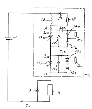
Fig. 1 is a circuit diagram showing a semiconductor
valve according to an embodiment of this invention;
Fig. 2 is an operational waveform diagram on
turn-off of a semiconductor valve shown in Fig. 1; and
Fig. 3 is a diagram given in explanation of symbols
and waveforms on turn-off of GTOs.
DETAILED DESCRIPTION OF THE PREFERRED EMBODIMENTS
Referring now to the drawings, wherein like
reference numerals designate identical or corresponding
parts
- 6a -
2107934
throughout the several views, the embodiment of this invention
will be described below.
Fig. 1 is a circuit diagram showing a semiconductor
valve according to an embodiment of this invention. In Fig. 1,
1 is a D.C. power source, 2 is a semiconductor valve, 3 is a
load and 4 is a free-wheeling diode. The internal layout of
semiconductor valve 2 is constituted by two sets of series
connected semiconductor devices and their associated components,
distinguished by suffixes a and b. 11 is a high-speed
semiconductor device, abbreviated as HSSD in this specification,
having a self-extinguishing function but the symbols are the
same as for a GTO. 12 is a diode connected in anti-parallel
with the HSSD 11. 13 is a snubber capacitor. 14 is a snubber
diode. 15 is a snubber resistor. 16 is a valve reactor. 17 is
a diode. 18 is a resistor that dissipates the energy of valve
reactor 16.
The layout of the semiconductor valve shown in Fig. 1
is a circuit that is conventionally employed. However, in a
circuit of this type, this invention relates how to select a
semiconductor device for suppressing variation in sharing
voltages on turn-off a semiconductor device, without increasing
snubber capacitor capacitance. The sharing voltage refers to a
.,y: .
voltage in a semiconductor valve where the walue~~ncludes a
plurality of series connected semiconductor devices. The
sharing voltage of one semiconductor device is just a little
different from that of another device because the
characteristics of the two devices are different from each
other.
- 7 -
~,.
2107934
First of all, the operation of this circuit will be
described using Fig. 1 and Fig. 2. Let us consider the process
whereby HSSDs lla and llb are turned off when a current IL is
flowing from D.C. power source through valve
_ 7a _
reactor 16 and HSSDs 11a and 11b to load 3. When an OFF
signal is applied to HSSD 11 at time tl, the current IL
flowing through HSSD 11 is divided into a current I11
flowing the HSSD 11 itself and a current Ic flowing through
the series circuit of snubber diode 14 and snubber capacitor
13. The currents I11 and Ic are also distinguished by
suffixes a and b, and currents Ills, Illb, Ica and Icb are
shown in Figs. 1 and 2. This current Ic charges snubber
capacitor 13. The voltage VAC between A and C shown in Fig.
1 is equal to the sum of the voltages of the two snubber
capacitors 13a, 13b, when it tries to exceed power source
voltage V, diode 4 conducts so that the circuit of load 3
and diode 4 is closed, allowing current IL to continue to
flow. Some of the current flowing through valve reactor 16
is branched to the circuit consisting of diode iT and
resistor 18, while the rest continues to charge up snubber
capacitor 13.
When
VAC - V = R.IL (where R is the resistance of resistor 18)
is reached, all of the current IL of valve rector 16 has
shifted to the closed circuit of diode 1~ and resistor 18
and charging of snubber capacitor 13 is completed. In
practice, due to the effect of stray inductance, not shown
in Fig. 1, snubber capacitor 13 is charged up slightly more,
_ g
21~~~~
but a discussion of this will be omitted as going into more
detail than is relevant to the explanation of this
invention.
In the waveforms in Fig. 2, the factor that affects the
sharing voltage of HSSD 11 is the ratio of the current
flowing in HSSD 11 and the current flowing in snubber
capacitor 13 from the time t1 up until the time t3. In Fig.
2, t1 is the time when an OFF signal is applied to HSSD 11,
t2 is the time when the turn-off time of HSSD il passes from
the time t1, and t3 is the time when the tail time of HSSD
11 passes from the time t2. In general, the capacitor
voltage is expressed by Q/C, where Q is the charge and is
the time-integrated value of the current flowing in the
capacitor, and C is the capacitor capacitance. If the
capacitance C of capacitors 13a and 13b is equal, the
variation in the voltages arises from the variations in the
magnitudes and times of the capacitor currents Ica and Icb.
Since the current I flowing through the series connection is
the same for both circuits of suffixes a and b, the cause of
variation in the capacitor current Ica and Icb lies in the
variation in the currents flowing through the interiors of
the two HSSDs; these currents are determined by the charges
in the interiors of the HSSDs. As explained earlier, thanks
to fine-processing, the turn-off time of the HSSD (time
between ti and t2 in Fig. 2, tgq in Fig. 3) is short, so the
degree of its variation in small. However, the tail time is
_ g _
not shortened by the miniaturization, so this comes to give
rise to the variation in the currents. For example, if the
variation in the tail currents of HSSDs of the 1000 A class
is assumed to be 20 A, and the tail times are equal at 50
as, the variation ~Q in charges Q is 20 A.(50/2) - 500
microcoulomb. If the snubber capacitance is assumed to be
0.2 uF, the variation OV in the voltages is, oV = 500/0.2 =
2500 V. For a 5000 V device the allowed value of the
variation OV is at most 500 V, so a snubber capacitor
capacitance on the order of 1 uF must be chosen; this makes
it impossible to raise the switching frequency. In this
invention, therefore, the variations in the tail charges
(this term is defined here for convenience as meaning the
charge which is discharged as tail current during the tail
time) is taken as the device selection criterion in series
connection. For example, in the case described above, if
the variation in the tail currents is taken as no more than
4 A, by a similar calculation the snubber capacitor
capacitance is 0.2 ,uF and the variation ~V is 500 V.
Thus, according to this invention, sharing voltage can
easily be contained within an allowed value without
increasing snubber capacitor capacitance by selecting the
semiconductor devices such that the variation in tail charge
on turn-off of the semiconductor devices is within a
prescribed value, so high-speed ON/OFF control of the HSSD
can be achieved.
- 10 -
~~o~~~~.
As a quantity with respect to the tail charge, a tail
current or a tail time may be used independently for
selection criteria of series-connected semiconductor
devices. It is also possible to take the ON voltage as a
selection criterion. Specifically, the ON voltage is
correlated with the number of carriers within the base
region; the voltage drops as more carriers accumulate.
Selection of devices for series connection can therefore be
performed taking as criterion the ON voltage when a certain
reference current, gate and temperature conditions are given
(In the case of transistor operation this is called the
saturation voltage. As used herein, the term "ON voltage"
includes this.)
Also, although in the semiconductor valve of Fig. 1 the
number of semiconductor devices connected in series was 2,
this number can have any value from 2 upwards. In this
case, as the variation in the tail charges on turn-off of a
plurality of semiconductor devices, a difference between a
maximum value and a minimum value of the tail charge on turn-
off of the semiconductor devices may be used.
Furthermore, in this invention the situation regarding
presence or absence of anti-parallel-connected diode 12 and
the type of snubber circuit is not restricted to that shown
in Fig. 1. The circuit to which the semiconductor valve is
applied is not restricted to that of Fig. 1. Furthermore,
GTOs or IGBTs which have been further improved are to be
- 11 -
included as HSSDs.
As described above, according to this invention, in
performing series connection of HSSDs, the variation in the
sharing voltages on turn-off can be suppressed to a
prescribed value without increasing the snubber capacitor
capacitance by taking at least one of the quantity with
respect to the tail charge including the tail charge, the
tail current, the tail time and the ON voltage as selection
criterion. As a result, there are the considerable
industrial benefits that the increase of loss and
deterioration of controllability resulting from increase in
capacitor capacitance can be prevented and that productivity
can be raised.
Obviously, numerous modifications and variations of the
present invention are possible in light of the above
teachings. It is therefore to be understood that within the
scope of the appended claims, the invention may be practiced
otherwise than as specifically described herein.
- 12 -