Note : Les descriptions sont présentées dans la langue officielle dans laquelle elles ont été soumises.
~o~
APPARATUS AND METROD FOR DEGOLDING OR TINNING CONDVCTIV~
PORTIONS OF A MICROELECTRONIC DEYICE
BACKGROUND OF TH~ I~VENTION
1. Field ~f the invention
The present invention relates to an apparatus for
processing a microelectronic device and in particular to an
apparatus for degolding or applying tin solder on electri-
cally conductive elements arranged on a face of the device.
2. DescriDtion of the related art
In solder processing of electronic parts it is known
that pre-tinning before soldering is necessary and that
fresh pre-tinning is preferable to the electro-deposition
techniques.
In the processing of microelectronic devices such as
chip carriers, it is known to remove gold and/or to tln the
conductive elements on a device face by dipping said face in
a solder melt. Several processes are known for removing
excess of tin : shocks or soaking the device in oil, or
spinning the device about an axis perpendicular to said
face.
The solder melt is at medium temperature recommended
by the process and standards (230C as an example), and the
solder material which is withdrawn by the device cools down
rapidly after the separation. Accordingly, in order to
achieve a solder deposit of regular thickness on the
conductive elements, and to efficiently eliminate the molten
solder remaining on the non-conductive portions of the
device, it is desired to start the spinning operation as
soon as possible after the conductive elements are separated
from the melt, i.e. after the meniscus between the devlce
face and the melt breaks. However, the level of the solder
melt is not known accurately when a series of devices are
2109~61
processed successively because an amount of solder ls
withdrawn from the melt by each processed devlce, so that it
is difficult to determine when the spinning operation should
be started. It is possible to attach a level sensor to the
device holder for detecting the melt level and controlliny
the splnning operation in response thereto. However the
operation of such sensor implles specific signal transmis-
sion and processing means and delays the be~lnning o the
spinning step.
SUMMARY OF THE INVENTION
It is therefore an ob~ect of the present invention
to improve the above-discussed apparatus in order to achieve
an accurate and reproducible melt level, so that appropriate
control permits the spinning operation to start as early as
desired after the separation.
According to the invention, there is provided an
apparatus for processing a microelectronic device having a
face with electrically conductive elements arranged thereon,
comprising a vessel for containing a solder melt, a bowl
having a horizontal upper rim for draw~ng molten solder from
the vessel, a device holder for holding the microelectronic
device with said face directed downwardly, and drive means
for moving the bowl and the device holder vertically with
respect to each other, thereby allowing said conductive
elements to be immersed in molten solder drawn by the bowl.
The upper rim of the bowl has an upwardly directed acute
angled edge extending therealong.
Initially, the bowl is completely immersed in the
melt. The surface of the liquid is cleaned by sweeping the
lighter surface oxides aside. Then the bowl is lifted to a
position where at least the upper rim is located above the
melt level. The edge along the upper rim promotes the rapid
formation of a meniscus between the molten solder and the
bowl wall. In addition, it ensures a clean, accurate and
` ~
6 ~ 1
.
reproducible level of molten solder in the bowl. The device
face can be immersed in the solder drawn by the bowl, and
then separated therefrom. The instant of separation is very
well determined due to the accuracy of th~ solder level.
Immediately after separation, the device is spun with a
profile of an~ular acceleratlon, maximum angular veloclty
and angular deceleration so selected as to leave the desired
solder thickness on the conductive elements. The machlne
allows the tinning process to be undertaken in gas media
(e.g. dry Nitrogen is frequently used).
Other objects, features and advantages of the
present invention will become apparent from the following
description of a preferred and non-limitative embodiment.
15BRIEF DESCRIPTION OF THE DRAWINGS
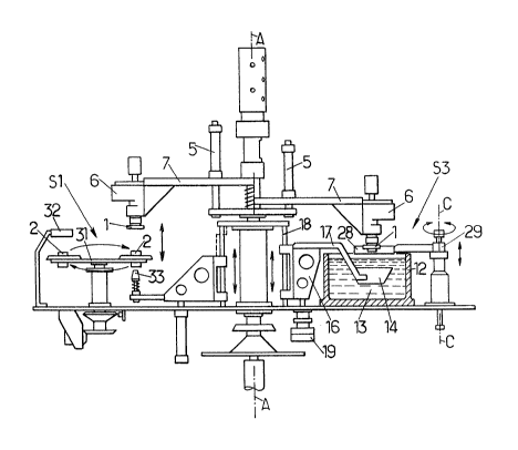
Fig. 1 is a top view of a processing installation
which lncorporates an apparatus according to the invention.
Flg. 2 ls a sectlonal vlew of the lnstallation of
20Fig. 1, according to the plane denoted as II-II.
Fig. 3 is an elevation view of a device holder of
this apparatus.
Fig. 4-6 are schematic views illustrating the
immersion of the device in molten solder.
25Flg. 7 is a view simllar to Fig. 5 in the case of
another type of mlcroelectronlc device.
Fig. 8 is a timing diagram which illustrates a
spinning step accomplished by the apparatus according to the
invention.
~ESCRIPTION OF A PREFERRED ~MBODIM~NT
The installation shown in Fig. 1 is used for
applying solder on conductlve elements of a microelectronic
35device. The installation comprises a plurality of stations
whlch may e.g. be dlsposed ln a carousel configuration, i.e.
a preheating and loading station Sl, a degolding station S2,
a tinning station S3, and a cooling and unloading statlon
S4. It will be apparent to those skilled in the art that the
installatlon may comprise other known stations such as a
fluxing station.
The installation comprises a device holder 1 for
holding the microelectronic device 2 and moving it from
station to station. The device 2 has a face 3 with conduc-
tive elements 4, e.g. contact pins, arranged thereon. As
best shown in Fig. 3, the device holder 1 is adapted to hold
the device 2 with the face 3 directed downwardly. Various
holding modes are suitable, for instance using suction
means. In this case, the holder 1 is a nozzle so configured
as to match the device shape, thereby ensuring an accurate
positioning of the device. Alternative holdlng modes are by
means of adhesives, magnets or electromagnets.
The device holder is mounted on a bracket 6 which is
secured to a horizontal support 7 rotatably mounted about
the carousel axis A (Fig. 1 and 2). An actuator 5 ls
connected to support 7 for moving it between an upper
position shown in the left-hand portion of Fig. 2 and a
lower position shown in the right-hand portion of Fig. 2. As
shown in Fig. 3, a first motor 8 is attached to bracket 6
for moving the device holder 1 along a substantially
vertical axis B, and a second motor 9 is provided, together
with an appropriate transmission 9a, 9b, for rotating the
device holder 1 about axis B at a controllable velocity.
The tinning station shown in Fig. 1 and 2 comprises
a vessel 12 for containing a Sn - Pb solder melt 13, and a
bowl 14 which is slidably mounted along a vertical direc-
tion. The bowl 14 is attached to a bracket 16 via an arm 17.
The bracket 16 is guided along a vertical rod 18, and
connected to an actuator 19 for obtaining the vertical
displacement of bowl 14. The vessel 12 is associated with
heating means (not shown) for heating the solder material to
a selectable temperature higher than its melting point.
~10~
The upper rim of bowl 14 extends in a horizontal
plane. As shown in Fig. 4-7, this rim has an upwardly
directed edge 21 extending therealong. The edge 21 forms an
acute angle of from 15 to 60 . In the illustrative embodi-
ment, this angle is about 45. The upwardly directed edge 2iis formed at the intersectlon of the lnner surface 22 of the
bowl and a tapering surface 23 of the bowl which extends
downwardly between said edge 21 and the outer surface 24 of
the bowl.
In operation, the device holder 1 is first brought
above the loading station Sl in order to grip the microelec-
tronic device which has previously been preheated. Station
Sl comprises a horizontal rotating support 31 for supporting
devices to be processed. The device 2 is first heated by a
radiant element 32, then transferred at the loading place by
rotating support 31. There, a vertically slidlng push rod 33
gently lifts the device 2 into contact with the devlce
holder 1. A depressurization of about 150 mbar is then
applied to the latter for firmly holding the device.
Then the support 7 is rotated to bring the device at
the degolding station S2 where it is prepared for the
tinning step. Thereafter, the support 7 is further rotated
to bring the device above vessel 12 at the tinning station
S3, and lowered by actuator 5 to bring the device closer to
the solder melt, as shown in the right-hand portion of Flg.
2.
At this moment, bowl 14 is lifted via actuator 19
from a position where it is completely immersed in the
solder melt 13 contained in vessel 12, so that at least the
upper rim of bowl 14 emerges from the melt. Accordingly,
bowl 14 draws an amount of molten solder from vessel 12. The
tapered shape of the upper rim of bowl 14 ensures a rapid
formation of the meniscus 26 (Fig. 4-7), and an accurate
positioning of the solder level in bowl 14.
The conductive elements 4 of device 2 are immersed
into the molten solder drawn by bowl 14. The immersion i~
~1~9~
performed by moving bowl 14 and device holder 1 vertically
with respect to sach other vla drive means which include
either motor 8 for further lowerlng the device holder or
actuator 19 for lifting the bowl, or both. Once the molten
solder has spread over the conductive elements 4 (Fig. 4),
the device holder 1 is lifted (and/or the bowl ls lowered ;
see Fig. 5) up to a position where the conductive elements
4 are separated from the molten solder (Fig. 6). As soon as
the latter position is reached, motor 9 is energized to
cause device 1 to spin about axis B. The rotational velocity
profile, i.e. the values of the angular acceleration,
maximum angular velocity and angular deceleration, is so
adJusted as to obtain the desired solder thickness on
elements 4 and eliminate the undesired solder on non-
conductive portions of the device. Such a profile islllustrated ln Fig. 8. The acceleration value (i.e. the
slope of the curve in the acceleration phase), the maximum
velocity V~, the duration D of the spinning at Vm~ and the
deceleration value (i.e. the slope of the curve in the
deceleration phase) are selected by the operator depending
on the nature of the conductive elements, the characteris-
tics of the solder (composition, temperature ...), the
desired solder thickness ... . As shown in Fig. 1, the
installation comprises a keyboard 36 for entering these
parameters and a computer 37 to derive the rotational
velocity profile therefrom and to control motor 9 accordin-
gly. Typical values of the maximum angular velocity V~ are
between 1 000 and 16 000 rpm, the angular acceleration and
deceleration being from 1 to 300 rounds per square second.
The relative positions of device holder 1 and bowl
14 when the device is separated from the molten solder are
well determined owing to the accurate positioning of the
solder level in bowl 14 which results from the shape of its
upper rim. Accordingly, appropriate control of motors 8, 9
and actuator 19 makes it possible to start the spinning
operation as soon as desired after the separation without
9~6~
requiring a special level sensor and the associated signal
processing.
Subsequently, the support 7 is further rotated to
bring the device at the cooling and unloading sta~ion S4
where it becomes available for further processing.
Fig. 7 is a view similar to Fig. 5 in the case where
the conductive elements of the device are metallized pads 4'
lnstead of contact pins 4. In thls case, the separation of
the conductive elements from the molten solder (i.e. the
break of the meniscus 27 between the solder surface and the
lower face of the device) may occur when the devlce holder
1 is at a different height with respect to the bowl 14.
Accordingly, it will be useful to consider the type of
microelectronic device to be processed when determining the
timing of the spinning operation.
A~ shown in Fig. 2, the tinning station S3 also
includes a horizontal blade scraper 28 which is fixed on a
rotatable support 29. When the support 29 is rotated about
a vertical axis C, the blade scraper 28 slides along the
surface of the solder melt 13 contained in vessel 12. This
sweeps a top layer of the solder melt 13 away from a surface
region located above bowl 14 when the latter is completely
immersed in the melt 13. This sweeping movement is performed
before bowl 14 is lifted by actuator 19, in order to remove
tin oxide which may otherwise be drawn by the bowl together
with the underlying solder.
The degolding station S2 may be used, if necessary,
for removing a gold film which is provided on the conductive
elements of some microelectronic devices for protective
purposes. In such circumstances, it is desired to remove the
gold film before the tinning step because gold and tin are
known to form a compound which is detrimental to the quality
of subsequent solderings. The "degolding" step may be
effected before the tinning step by means of station S2
which is identical to the tlnning station S3. The device i~
dipped into a solder melt, separated therefrom and then
~103~
spun. The spinning step i~ similar, with a different choice
of angular acceleration, rotating velocity, duration and
angular deceleration, in order to virtually ellminate the
solder containing traces of gold. The next statlon is the
tinning station S3 where the device is processed as descri-
bed hereinbefore.
As shown in the top view of Fig. 1, the support 7
preferably carries a plurality of brac~ets 6 and device
holders, whereby the processing rate can be enhanced. In the
exemplary embodiment, four brackets 6 are provided on the
carousel support 7 (one of which is not shown in Fig. 1 for
exposing vessel 12 and bowl 14 at the tinning station S3
at regular intervals so that the four device holders can
stay simultaneously at a respective station.
The invention has been disclosed with reference to
a preferred embodiment. However, it wlll be readily apparent
for those skilled in the related art that many alternative
features may be contemplated without departing from the
spirit and scope of the inventlon.