Note : Les descriptions sont présentées dans la langue officielle dans laquelle elles ont été soumises.
W~92/22~38 2 ~ 1 0 ~, ~ 7 PCT/U~92/0427~
RETROREFLECTING POhARIZER
5 Technical Field
This invention relates to polarizing thin film
stacks coated onto substrates having structured
surfaces~
lo Back~round
A MacNeille polarizer ~omprises alternating
repeatiny layers of a pair of thin film materials
deposited on a bulk substr~te material. The pair of
thin film materials comprises one low refractive index
I5 material and one high refractive index material. The
indices, called a MacNeille pair, are chosen such that,
for a given angle of incidence of a light beam, the
reflection coefficient for p-polarized light (rp) is
essentially zero at each thin film inter~ace. The
20 angle at which rp is zero is called the Brewster angle,
and the formula relating the Brewster angle to the
numerical values of the indices is called the MacNeille
condition. The reflection coefficient for s-polarized
; light (r9) is non-zero at each thin film interface.
25 ~Therefore,~ as~mo~e~thin film layers are added, the
total reflectivity~ for ~-polarized light increases
while the~reflectivi~ for p-polarized light remains
essentially~zero. ;Thus, an unpolarized keam of light,
inciden~ upon th~thin film stack, has some or all of
30 the~s-polariæed compQnents reflected while essentially
all of the p-polarized component is ransmitted.
; Such a~thin~film~stack is deposited on two general
; types~of substrates, which~then classifies the type of
polarizer~ produced as either immersed or non-immersed.
35~For~example, if the thin films are deposited on a flat
face which~forms~the hypotenuse side of a right angle
: `
::
Wi~92/2283~ 7 PCT/US92/04271
-- 2
(Porro) prism, and bonded to the similar side of an
identical prism, the polarizer is an immersed
polarizer. If the thin films are bonded between two
planar slabs of transparent media, the polarizer is a
5 non-immersed polarizer. In general, a polarizer is
non-immersed if the geometry of the bulk encapsulant
does not affect the immersion constant nj*sin(~;) of the
light beam in a thin film material ~.
For either immersed or non-immersed polarizers,
lO the p-polarization component of an incident light beam
is transmitted, while the s-polarization component is
reflected from the thin film stack at a~--angle equal to
: the angle of incidence. The total change in direction
of the s-polarization component from the incident
15 direction is goo for cube polarizers and usually about
60 for slab polarlzers. Thus, the s-polarization
component is typically unavailable for further use,
leading to a decrease in overall intensity of light
ava~ilable, un:less ~dditional optics are employed to
20 :~re:direct: the s-polarization compon~nt. For example,
U~.S. Patent 4,9I~3,529 (Goldenberg et al.) discloses a
liquid crystal display (LCD) television projection
system~using two~re:flectors, a polarization rotator and
,, , ~
a prism~to recombine:both components.
25~ Such~systems are~ undesirably large for use in many
common:visua:l:display~systems, such as overhead
proje~ctors, and~especially;:in portab~e or laptop
computer displays~where~a ~hin profile is desired.
30 ~Disclosure o~ Inventlon~
I The invention is a retrore~lecting polarizer,
compr~lsing~
(a)~a first~materia~l having a structured surface
35 consisti~ng of a linear array of substantially right
angled isosceles pri~sms arranged side by side and
~,
W~92/22838 ` 2 1 ~ ~ 3 ~ 7 PCT/US92/04271
- 3 -
having perpendicular sides which make an angle of
approximately 45 with respect to the tangent to a
smooth surface opposite the structured surface,
(b) a second material essentially like the first
5 materi~l,
(c3 on the structured surface of at least one
material, at least one optical stack of alternating
layers of high and low refractive index materials of
se1ected optical thicknesses; the first and second
~0 materials all opti~ally cemented to form a single unit
in which the refractive index of the first and second
materials, and the refractive indices and optical
: thicknesses of the layers of the optical stack, are all
:~ chosen to produce seIective reflection of polarized
15 light, such that:
(d~ wit~in one portion of the optical stack, an
incident light beam of mixed polari~ation is separated
into an s-polarized component and a p-polarized
component,
: ~ (e) the s-polarized:component is reflected onto
another portion of the optical stack and there
reflected paral:lel to~the incident beam but proceeding
~ :
in an opposite ~irection, and
(f~ the p-polarized component is transmitted
25 parallel to:the inciden~beam.
Brier Descript1on_of~ehe DrLw-In~
Figure ;l~is~a cross~sectional view of a portion of
one~preferr;ed~e~m~odiment~of: ~he :~invPntion .
~ Figure 2 is:an~:enlarged sectional view of a
port;ion oflthe embodiment of Figure l.
Figure 3;is~a~;:schematic side view of an optical
:system employing the invention.
: Figure 4 is a graph~of the transmissivity and
:35 :reflectivity of light incident upon one embodiment of
: the invention.:
::
W092/22838 ~ 1 1 0 ~ 0 7 4 _ PCT/US92/04271
Detailed Description of the Invention
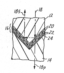
~ igures l and 2 show an inventive retroreflecting
polarizer lO, comprising two pieces of transparent
substrate material 12 and 14, between which is is a
5 composite optical stack 16.
The pieces l2,l4 each have structured surfaces
(which face each other), and non-structured surfaces.
As shown, piece 12 is a top layer and piece 14 is a
~ubstrate, but the entire assembly may be inverted with
l0 no loss of functionality, essentially interchanging the
:~ roles of the two pieces.
In the embodiment shown, the composite optical
stack 16 is deposited upon the structured surface of
~: the upper piece 12, and the structured surface of the
lower piece l4 is:optically cemented (i.e., adhered by
a very thin layer of transparent adhesive) to the
composite optical stack 16 by an adhesive 24 to form a
single unit. However, the composite optical stack
: :could comprise two~:sub-stacks, one sub-stack deposited
20 on the~top layer and the other deposited on the
substrate, with adhesive 24 betw~en the two sub-stacks.
The composite~optical:stack compri~es at least one
se~ of~:~pairs of alternating layers of materials having
low~and~high~indices~:of~refra~ction compared to each
25~other.~ The~thicknesses of the layers are chosen such
that the~quarterwave~criterion:is met for the
wavel~ngth o:f~the incident collimated light beam 18 by
each;o~ layers~20~;and 22. ~ The~shape of the structured
surfaces,~thé~optlcal properties of the substrate
::30:;material,: and~the~:properties of the composite optical
stack,~all,:combine to~di~ide~the incident light beam
into~wo polarization components. One co~ponent, 18-s,
is refl:ected:;twice~in:such a manner as to be
retrorefle~ted, i~.~e.~,~ directed back toward the source
35 of ligh~beam 18. ~The other component, 18-p, is
- transmitted paral~lel to lncident beam 18.
211~ 7
W092/22838 PCT/U~g2/~271
(In Figure 2, the division of incident light 18
into components 18-s and 18-p is shown as occurring at
the first interface between the substrate and the
composite optical stack, but this is illustrative only.
5 Actually, some division occurs at each interface
between thin films, with the net result being as
shown.)
In the embodiment shown, the composite optical
stack comprises a repeating stack of a pair of
: ~ 10 materials. One of the materials is a relatively low
refractive index (nL) material 20, and the other is a
relatively high index (nH) material 22. The
construction of such a stack 16 is abbreviated (HL) 2.
In general, more layers are u~ed, such as a (HL3s sta~k,
~:~ 15 and generally the average optical thickness of each
material is a~quarterwave thick, with reference to a
chosen wavelength::of interest (typically but not
necessarily in~the~visible spectrum). However, to
optimiz:e performan'ce, the:individual thic~nesses of all
Z0;~thin~fi~lm layers are~varied 'slightly from the average
~ thick~ess, in~accordance with known principles, using
";~ :commercially available~:software:to calculate the
desired values.~
Also,~more~:than~two~pa:irs of materials or average
,2~5~thicknesses;mày~:~be~used,;such~as a (H~LI)5~(H2~)5. This
would~be~:~one to~extend:~;the useful optical bandwidth of
the~invention~'or~`the~range:of-angles over which the
vention~reflects,~essentially~all s-polarized light.
~3~ Each~;of~substrate~pieces~12~and 1:4 comprises a
: : 30 ~transparent,:~:p~e~féra~ly integral ~(i.e., a single
dontinuous~lpiece~as opposed to an assembly or a
laminate)~:material~having a~structured surface which
:consists of:~a;~linear~array~of~substantially right
,angled~ sosceles~:prisms~arranged side by side. The
35~;~perpendicular;:sides~of~each prism make an angle of
- approxim:ately:'45 with~ respect t~ the smooth surface
W092/22838 2 i ~ 7 PCT/~S9~/042?l
-- 6 -- .
opposite the structured surface (or~ in the most
general case of a flexible substrate, with respect to
the tang~nt to the structured surface). Angles other
than 45 are useful for other applications, but angles
5 near 45 (e.g., ~0 to 50) are preferred in this
invention. This places a constraint on the design of
the optical stack: only two of the three indices of
refrartion (nL and nH for the optical stack, nO for the
:~ ~ubstrate pieces) can be chosen independently. (An
10 additional implication is that nL must always be less
than nO if high transmission of p-polarized light is
desired at all wavelengths.) These values are
;~ determined by the MacNeille condition relating the
Brewster angles of each material interface to the
15 numerical values of the indices of the materials
forming the interface: ;
tan(~L) = -(nHlnL~
or,
: tan ( ~H) = (nL/n~)
; al~ong~with Snell~'s;~law~relating~0 to ~L and ~H.
: 25 ~ In;theory, an~infinite set of values of nH and nL
exist~f~or~a given ~nO~ :~but in practics, the available
choi~es~:~of mater:ials~;~for the substrate pieces and thin
films~are~`~limited~ and~design of the invention reduces
to~:choosing~whi~ch o~the limi~ed set of values of nH
30 ~and nL~:~around~th~at::`value::of nO will produce the desired
results.~ IThe~gre~ater the dif:ference between nL and in
the wider~the~ optical~bandwidth over which the
invent~ion will divide incident light into separate
polari~zations. :;:
35~ ~ A:suitab~le thickness of the substrate is 0.36
millimeters, ~éa~sured from the smooth surface to the
:: ~
W092J22~38 ~ U 3 ~ 7 PCT/US92/04271
lowest point of the grooves. Suitable groove heights
(measured perpendicularly) are 0.18 mm. For such a
film, about 28 peaks per centimeter is preferred, but
there is wide latitude in the dimensions.
Preferred substrate materials are flexible,
homogeneous, and isotropic. Suitable materials include
commercially available acrylics and polycarbonates
ha~ing nominal indices of refraction of 1.49 and 1.59,
respectively. Other possible materials, selected to
10 provide the required functionality, include
; polypropylenes, polyurethanes, polystyrenes, and
polyvinylchlorides. Generally, polycarbonates are
preferred for their relatively high indices of
refraction, clarity, and physical properties.
Higher index materials include polysulphone (and
variations such as polyethersulphone and
polyarylsulphone), polyethylene teraphthalate ~PET),
and polyethylene napthalate (PEN). The sulphone~
reguire high processing temperatures, but in turn can
20 withstand higher ambient~temperatures in use. PET and
PEN may~rystallize or exhibit~bir~fringence depending
on the process~parameters~. All these materials ha~e
indices ~in~the range~ of 1~63 to 1.65, and as such~
allow~th;e use~of~the~film pair~SiOJTiO2 while retaining
2~9~ high~transmission~0f~p-polari~zed~light.
A suitable material is taugh~ in U.S. Patent
4~805~ 984~(Cobb,~ 3r.3~,~ but in~this invention the total
internal~ reflection~property of~that material is not
rel~vant,~because~he~optical properties o~ the
30;~ material;~are~signiflcàntly ~hanged when it is employed
in this~;invention. ~
Suitable materials for the~thin films 20 and 22
include any~materials~which are trans~arent (exhibit
19w~ absorption~in the~spectrum~of interest. For
- 35~ bro~dband visible 1ight, suitabl~e thin film materials
are silicon dioxide;~SiO2) (n=1.45); amorphous
W092/22838 2 1 1 ~ ~ iJ 7 PCT/US92/~271
hydrogenated silicon nitride (a-SiN:~) (n=1.68-2.0~;
titanium dioxide (TiO2) (n=2 . 2-2 . 5); magnesium fluoride
~MgF2) (n=1.38); cryolite (Na3AlF6) (n=1~35); zinc
sulphide (ZnS) (n-201-2.4); zirconium oxide (ZrO2)
(n=2.05); hafnium oxide (n=2.0); and aluminum nitride
(n=2.23. Silicon ~itride (Si~N43 is suitable, but has
not been furmed successfully on the preferred
polycarbonate:substrate.
Several thin film deposition techniques can be
10 used t~ deposit the composite optical stack on the
substrate. Thermal and electron beam evaporation, and
ion beam sputtering are the methods of choice for
precision optical coatings, the latter method producing
superior films in terms of adhesion to the substrate,
:15 hardness, and~environmental stability. Magnetron
i sputtering is also used extensively for broadband
coatings such as anti-reflective coatings on glass, and
especially ~or~large area applications such as
architectural:glass. However,~on the whole, thermal
: 20 and electron beam evaporation should provide good thin
film ~ualities and~suf~iciently high deposition rates
for~`acceptable manuf~acturing rates. More importantly,
low index:films such~:as magnesium fluoride and cryolite
can~be~deposit~d~by;this method.~ Electron beam
2s deposition is~;regular~y~used~in the coatings industry
or hi;gh~index~materials such as titanium dioxide,
zirconium oxide~,~:hafnium oxide:, ~nd aluminum nitride.
The~pro~èss~used~:in the reduction to practice of
the~invèntion~was~plasma assisted chemical vapor
::: 30 deposition (PAC~D).~ Using this PACVD, the following
proceduresj~and resultant products~,are possible.
SiO2~may~be~deposi*ed by reacting silane (SiH43 or
almost`any:organosilane;~in the~PAVCD process with
oxygen~or nitrous oxide at between 50 and 250
35~ milliTorr, using~l:ow power RF plasmas of about 50-100
watt/ft2 of e~lectrodè area. Nitrous oxide is somewhat
:::`: :` :` ~
'r~ C~ ,X.~ ;r~ ;rr~ s;r~ 5~ r~,-r~,r"~ ~,".~ ",~; ;"-5-~;--q .
wo g2/22838 2 1 :I Q 8 ~ 7 PCr/USg~ 271
.;'
g
preferred because it generally results in less powder
formations in the gas phase.
Tio2 may be formed by reacting titanium
tetrachloride (TiCl4) with oxygen and nitrous oxide at
5 the same power levels. By varying both the rela~ive
and absolute flow rates of the 02 and ~2 for a given
flow of TiCl4 vapor, the index of refraction of the film
is easily varied/ from 2.0 to 2.4. Residual chlorine
in the film can result in poor adhesion to
10 polycarbonate. An oxygen flow of several times in
excess of the reactant gas is preferred.
The visibly transparent a-SiN:H material has an
index of refraction which varies mainly as a function
of deposition temperature, with the higher indices
15 requiring temperatures of 250 Celsius or mo~e. The
films may be deposited from mixtures of silane,
ammonia,~and nitrogen. Films formed at lower
temperatures from conditions suitabl~ for high index
films:(i.e., silane, starved nitrogen, no ammonia)
20 produce undesirably high absorption of blue light. It
is possible to form films having indices between 1.68
and 1.8 on polycarbonate below 100 C, with low optical
absorpt~ion, although `the lower index films are somewhat
brit~le. ~ ~ ~
~ . ~
The PACVD~process was carried out usiny a
deposition~:system~according to:the teachings of U.S.
Patents 4,841,908~and:~4,874,63~1 (Both Jaco~son, et
al.~3. ~Briefly, this; multi-chamber deposition system
employs~:a~;~large:volume vacuum chamber within which are
30:plurality:0f deposition chamb rs for different
composition layers, each chamber having separate seals
to minimize back diffuslon of~any dopant gases from
adjacent deposition chambers. A:continuous roll of
: substrate proceeds from a supply roll through each of
35 the deposition chambers and onto:a finished take-up
roll. The direction of web travel is reversed
~: :
w~g~/2~38 ~ 3~ a7 - lo - PCT/US~ ,271
repeatedly to produce the multiple layers of repeating
re~racti~e index materials.
The index of refrackion (nA) of the adhesive 24
should match that of the upper and lower pieces 12 and
5 14 as closely as possible. When the index of the
adhesive is less than that of the adjoining piece, the
non-zero thickness of the adhesive leads to some
refraction of light away from the original beam
~: direction. Adhesives of nA = 1.56 are available from
:: 10 the Norlund Company. Suitable adhesives are Norlund
numbers 61 and 81 optical cements (nA = 1.56~. Another
:~ ultraviolet curable resin (nA = 1.50) can be made from
: Union Carbide number ERL 4221 epoxy resin with 1% (by
: ~ weight) Minnesota Mining:and Manufacturing Company
~; 15 number 41-4201-91185 sulphonium salt initiator. The
initiator is dissolved in methelene chloride which must
: be evaporated~ off before mixing with the epoxy. Other
W curable mixtures, not as preferred, may be made from
urethane acrylate ba~Se resins, diacrylate diluents, and
20 suitable photoinitiators. ~W :::curable adhesives may
cause~slight:~absorption,~ mainly~in the blue end of the
spect~um, in the completed~polarizer of about 1-2~.
: Any~the~mosetting~adhesive or epoxy will work also
provided~It~ha- Iow~optica1 absorption and high index.
Example~
A1ternating~thin~fi1m layer~s of matched
quar~erwave~optica~ thickness were coated on the
:structured:side~:of~a~14:mi1 thick polycarbonate version
30~o:f the~preferred~substrate material;:described in U.S.
Patent 4,805j98~4~(;Cobb, Jr.) In Example 1, ~oating
wa~s:~done~by::;the~plasma~assiste~ chemical vapor
deposition (P~VD)~process~desoribed above, using a 5
.inch~wide and 8 inch~long gas "showerhead" type
35 electrode. To:form~the~retroreflective polarizer, an
~ ~:
W092/22838 PCT/US92/0~271
, . . .
uncoated piece of the TIR material was adhered to the
optical stack with an optical adhesive.
In Example 1, the polarizer had three optical
stacks ! each having twelve layers, either silicon
5 dioxide (SiO2) or titanium dioxide ~Tio2). The
unusually high number of layers was required because
the PACVD technique as described above did not produce
a uniform film thickness near the prism peaks as
opposed to the bottoms of the grooves. The first stack
10 had a quarterwave thickness centered at 400 nm, the
next centered at 550 nm, the third centered at 700nm.
The polarizer performance is shown in Figure 4.
Transmissivity of the s-polarization component, T(s),
was at or near zero throughout nearly all tha visible
15 spectrum~ while reflectivity of that component, R~s),
approached the 95% level typical of the most efficient
;~ common~reflectars. Transmissivity of the
p-polarization:component, T(p), was very acceptable,
nearly 80% or more throughout the~visible spectrum.
It is useful to provide a few details of the
angular dependence of the~retroreflecting polarizer.
, ~ :: : : ~ :
The:first feature :is the~ angular dependence of
t~ansmission~for~p-polarized light, through one prism
facet.~The;ang1e~theta~is~measured in air from the
: 25 unit vector normal to:the outside surface of the
retroréflecting~ polarizer.~ The~assumed ~ilm stack is a
combination~-of;three stacks~designed to cover the
visi~le~spe~trum:at~all~angl~s of incidence. The
transmis~sion~speotrum~vs. ~angle:~is broader at lvnger
30 wa~elengths (+45 at 650 nm).~ This stack comprises
twenty-eight layers::;an eight layer stack centered at
6:00 nm~and;45 (immersed)~, along. with a double stack,
of ten:layers each,:designed fo~ 15, with center
waYelengths of 450:~and~600 nm.
; 35 ~ The computer: calculated angular dependence of
transmission, ~for a wavelength of 450 nm, shows an
assymmetry of p-polarized transmission for positive and
:: :
W0~2/Z2838 PCr/US92/0~271
2i1 f~ J7 - 12 -
negative values of theta. This arises from the
inclination of the prism facets at 45 from the
substrate surface, wheraas the angle theta is measured
in air from the norm,al to the outside surface. Total
5 transmission through the polarizer is the sum of two
transmissions, at com~limentary angles, through ~wo
opposing facets. When both terms are taken into
account, the transmission curve is symmetrical.
Tertiary and higher order reflections from light
10 transmitted laterally at the second prism can be
accounted for as well, but do not have a great impact
on the shape of the curve.
Applications
The invention is suitable for applications
requiring polarized light that would benefit from
increasing the ~intensity of the polaxized light
available from an unpolarized source, and especi~lly
those requiring polarized light over relatively large
20 areas and/or in~ relatively compact ~especially thin~
applications~
For example, the inventive retroreflecti~g
polarizer can be~ combined in a very simple manner with
a ~uarterwave~re~ardation;~plate and a refleGtor to
25 ~recombine~the~two~components o~an incident light b'eam
into ;a sing1e~polarized component~of light. Such an
; arrangement is~ hown~ln;~igure 3. A combined reflector
and~sour~ce~;of;~incident~light 118 is illustrated
schematical1y~as; 130~ Incident~liyht 118, having mixed
30~polarizat;ion,~is~not~affected~by~quarterwave
retardati~n~plate 120,~but is split into components
118-p~and~118~-s~by~retroreflecting polarizer 100.
Component 118-p~is transmitted~directly to display
device llO.~Component~ s is~retroreflected back
35~through a quarterwave~rétardation plate 120 as shown by
119, and ref~lected ~(and displaced transversely upward
~:
~ for clarity as~component 1213~back through the
:
2 1 ! ~' 3 ~ 7
W092/22838 PCT/U~92/~4~71
. ., .~
- 13 -
quarterwa~e retardation plate again as shown by 121.
The two passes through the quarterwave retardation
plate represent a total rotation of ~0, i e.,
component 118-s now has the same polarization dirPction
5 as component 118-p, and is also directed toward display
device 110, thus nearly all of the intensity of
incident unpolarized light ~18 is available in
polarized form at display de~ice 110.
The great advantage of the invention in this
~: ~ 10 system is that because all components may be relatively
~ thin and large in area, and lie on essentially the same
: optic axis, the profile of the system can be greatly
reduced. Where reduction in profile is not as much a
~: concern, or where convenient for other reasons, the
15 QptiC axis can be red:irected without loss of
generality.
Reflecting source 130 may be the light source of a
backlit computer display, or an overhead proje tor such
as models~widely available from the Minnesota Mining
20 and~Manufacturing Company. :Display:deviGe 110 may be a
qroup ~of one :or more birefringent LCD panels, employed
in monochrome or color applications~ such as those
disclosed~in;~U.~S. Pa~tents 4,917,465 (Conner et al.) and
4,966~,441 (~Conner)~
;25 ~For~this application:, assuming a polycarbonate
: substrate~o~ index::~nO = 1.~586,~:the~ideal thin ~ilm
: indices~are;~nH~ 2~ 0:and nL~=~;1.35. With this pair of
indices;~, the:theoretical minimum~:composite optical
:stack~for~a~;photoptic~ e.:,~ covering the entire
: 30 visible~spectrum)~retroreflec*ing polarizer is two sets
f~eight layers~ e~ HL)4+~(H~'L~)4. One set has a
bandwidth centered:on 425~nm~and~the other has a
b~andwidth~center~ed~on~650 nm. A1though cryolite has
the:most desired~low index (nL =~l.35), it is soft and
35 slightly hygroscopic,~so magnesium fluoride ~nL = 1.38)
is~preferred. :Z~irconlum oxide (nH = 2.05) is one
W092/22838 ~l~a8~7 PCI/V!i92/0427
-- 14 -- I
pref erred high index material, although several other
materials arP suitable.
:::
~,
: :