Note : Les descriptions sont présentées dans la langue officielle dans laquelle elles ont été soumises.
~~.:~~~~_~
11U'TEGRATED PARTIAL, SAWIhICy laltsD~ESS
Bt~CK~iR~ilhll~~ ~F THE II~IVEf~'fICDIV
1. ~~,1_d of the inv~ntinn
This invention relates to semiconductor processing, more particularly to saw
and cleaning
S operations.
2. Background of the invention
Multilayered devices, such as micromachin~;s, that are built on semiconductor
wafers are
becoming more common. Many of these require processing of sacrificial layers
or similar
processes that are better done while the individual chips are sfill in wafer
form.
However, many problems with contaminants and debris arise if the processing is
done
before dicing the wafer into separate chips. For example, if the wafer is
processed to remove
a sacrificial or protective layer used in the earlier stages of the process,
when the wafer is
divided into chips, debris from the division can come in contact with the
surfaces previously
protected or covered by the sacrificial layer.
1~ Another option is to divide the wafer first, then finish any processes that
remove
sacrificial or protective layers on the individual chips. Depending on the
process, and the
earners used for the process, this can be prohibitively time-consuming, labor-
intensive and very
expensive.
Therefore, there exists a need for a method or process that allows processing
to be done
in wafer form in such a manner to eliminate or limit contact between the
debris caused by. ...
dividing the wafer, while not requiring large amounts of time.
'TI-~7~66 Fage I
CA 02113019 2004-02-17
SUMMARY OF THE INVENTION
The present invention disclosed herein comprises a method of processing
semiconductor
wafers that eliminates contact between protected/covered surfaces and debris
from wafer
division. One embodiment of the method comprises mounting the wafer on a saw
frame,
partially sawing the streets between the chips on the wafer, covering the
streets with a protective
tape or caulk, completing the remaining processes on the wafer, breaking the
wafer, and then
picking and placing the individual chips off the saw frame.
In accordance with one aspect of the present invention there is provided a
semiconductor
process comprising: a. partially sawing streets on a wafer; b. covering said
streets with a
protective coating; c. processing said wafer; d. positioning a wedge piece
with a plurality of
wedges adjacent said wafer; e. applying pressure to force said wafer against
said wedges
causing said wafer to break into chips along said partially sawn streets; and
f. removing said
chips.
Page 2
i3RIEF DE;SGIZII''I'I~M OF THE DRA3NIhdGS
For a more complete understanding of the present invention and for further
advantages
thereof, reference is now made to the following Detailed Description taken in
conjunction with
the accompanying Drawings in which:
FIGURE I shows a flow chart of one embodiment from partial saw to removing
individual chips.
FIGURE ~ shows a flow chart of one embodiment for the protecting step of the
overall
flow
FIGURES 3a and 3b show an alignment for the placement of protective tape.
FIGURE 4 shows a side view of a wafer with protective caulking in partially
sawed
streets.
FIGURES Sa and Sb show a side view of a wafer on a saw frame with partially
sawed
streets and a possible breaking pattern for the wafer.
TI-I75S6 Page 3
/,.r ~_ ~ Rd ~~ '~ eJ
DETAILED DESCI&IPTIOhI OF THE PREFERRED E1~BODI1~IEI~ITS
Figure 1 shows an overall process flow 10 for a semiconductor wafer that can
be adapted
to use a protective tape or caulking in the streets between the chips. The
process starts after all
of the processes are completed that are specific to that micromachine or
multilayered structure.
For example, addressing circuitry or actuators may be put down or implanted
into the substrate.
Then a layer of polymer or other sacriFxcial material can be laid down on top
of the circuitry or
actuators. This layer can be hardened and processed to support posts or spokes
for
micromechanical strtactures that require freedom of movement from the actuator
layer. After the
supports are in place, the material for the active part of the micrornachine
follows. Whether or
not the ftnal layer is patterned or patterned and etched before beginning the
process in Figure
1 is a process choice left to the user.
Therefore, at the point in which this process will most likely be used, there
is a
mulrilayered semiconductor structure with its protective or sacrificial layers
intact, on each chip
on the wafer. The process in Figure 1 begins at step 12 with a partial saw or
diamond scribe
over the streets on the wafer. It may be desirable to put a removable
protective coating over the
entire wafer before sawing to further limit debris from the partial saw or
scribe from settling on
the important device features. The thickness of the material left behind in
the streets depends
on the substrate material, further handling constraints, and the process
designer's choice of
breaking apart the chips. When the actual sawing or scribing occurs, the wafer
will be mounted
upon a standard saw frame.
In step 14; the protective coating, if used, and the debris from the partial
saw, is removed
in a post-saw cleaning. The removal may be a wet process, depending on the
material used as
TI-17566 Page ~
w
a protective coat. One example could be a resist used as a protective coat
that is removed with
a wet etch. Tn step 16, the process returns to the processes specific to the
micromechanical
structure being fabricated. Typically, this process will involve removing the
sacrificial layer
thereby allowing the active elements of each machine to move freely.
Additional processes may
also take place to cover or protect various surfaces of the micromachines that
were not exposed
previous to removing the sacrificial layer, such as thin-film processes.
At step 18, one advantage of this process becomes readily apparent. The wafer
is soil
intact, so the die registration is very precise. Also, this step allows the
process operator to
determine yield by ascertaining which chips are operational, to be noted for
remaval later. This
can be accomplished on a standard mufti-probe station.
Step 22 in this diagram is stated very generally. An elaboration of the steps
within the
protection process of step 22 is shown in more detail in Figure 2. Two
possible options are
shown. Step 26 would begin at the completion of step 18 from Figure 1. A
material to be used
as tape is punched or cut with a pattern that matches the pattern of the
streets on the wafer. A
typical material could be mylar. The mylar would be treated with some typo of
adhesive, such
as a UV or low-pressure sensitive adhesive. Then the process moves to step 28,
in which the
tape is aligned and applied to the wafer, completely covering the already
partially sawn streets.
A graphic illustxaron of the alignment is shown in Figures 3a and 3b. In
Figure 3a, the
tape 4~ is shown with its pattern punched. There is a hole 46 for the die. The
grid represents
places where the taps is left intact. In Figure 3b, the dashed line 48
indicates the wafer's. ...
position after application of the tape.
In this embodiment, the wafer is then mounted on a frame for a commercially
available
T~-17566 gage S
wafer breaking machine in step 30. Further etaborations on a technique for
breaking will be
discussed in Figures 5a and 5b. Other possible embodiments could include
rolling the wafer
across the surface of a drum, breaking the wafer as it tries to bend to the
curvature of the drum.
During the breaking process in step 3Z, the tape over the streets traps any
debris from the
break and prevents it from contaminating the active parts of the
micromachines. Regardless of
which breaking technique is used, when the wafer is broken, the adhesive on
the wpe is
weakened, such as that treated with UV light, the tape is peeled away, and the
chips can be
removed by standard semiconductor machines which handle picking and placing of
individual
chips, in step 34.
An alternate method begins at the same point as the above process, just after
the
completion of step 18 from Figure 1. precision injection tools are fully
capable of applying a
protective material, such as a resist, to the streets in exact amounts. A side
view of a wafer with
caulking in partially sawn streets is shown in Figure 4. The wafer 48, has
partially sawn streets
50. The caulking material 52 is injected so as to not ovea-fill the streets
and appraach the edge
of the active areas of the chips. The Baulking material could then undergo a
soft-hard bake, in
which it is hardened far better structural integrity. Again, in this
embodiment, framing the wafer
for a commercial breaking machine is shown in step 38. When the wafer is
broken in step 40,
the caulking traps any debris that could have escaped and damaged the active
areas of the
micromechanical structures.
The material used as Baulking may be left in place, depending on material. The
required.. r
attributes for the material are that it does not generate any particles,
especially over time, and
that it does not outgas. These are important in all micromachines, but
especially important for
TI-17566 Page S
~.. .~ t.~ l
uptical micromachines that are exposed to intense illumination, such as
spatial light modulators.
Particles can cause illumination scatter and micromechanical obstruction. An
outgassed film can
collect on micromechanical surface and can increase the stiction
("stickiness") coefficient between
two surfaces. Additionally, if the micromachine is illuminated through a
window, such as some
closed-package spatial light modulators, the outgassed flm can lower the
illumination by
obscuring the window. One possible caulking material is a silicon-based
rubber.
After the chips are separated via a breaking process in step 40, the pick and
place tool
can remove the chips from the frame in step 42. This completes the protective
process for
certain methods of breaking. Another alternative method for breaking is shown
if Figure Sa and
Sb. The breaking step can be in the process shown in Figure 1, step 24, or a
part of an entirely
separate process that does not involve protecting the streets. The only step
from the process of
Figure 1 is the partial saw at step 12, or some equivalent thereof.
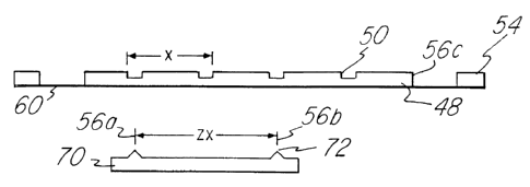
Figure Sa shows a side view of a wafer 48, on a saw frame S4. 'The wafer rests
on wafer
dicing tape 60, which could be any dicing tape typically used in semiconductor
processing.
Having completed all of the micromachine-specif-ac processing, the wafer must
now be broken.
It is not necessary that the wafer be protected as previously discussed,
although it would more
than likely be desirable. The distance between the streets is X. A wedge piece
70, comprising
a plurality of individual wedges 72, is used to provide a stress concentration
point and push up
at points every 2X on the scribe lines, shown at points 56a and 56b. The wafer
may also be
pulled down against the wedge by a vacuum from underneath the wafer. .. ...,.
The 'wedge will cause the wafer to break in the pattern shown in Figure Sb.
Chips 48a
and 48b will be separated by an upward break represented by the point 58a.
Chips 48b and 48c
TI--1756 Page 7
will be separated by a downward break represented by the point S8b. After the
wafer is broken,
the wafer protective tape is treated to reduce its tackiness, for example with
UV exposure if it
is L1V adhesive, and is removed. If a protective coating as discussed above
was used, it may or
may not be removed. Then standard semiconductor tools can be used to pick and
place the
individual chips off of the saw frame.
Although there has been described to this point particular embodiments of
wafer-form
processing for micromachines, it is not intended that such specific references
be considered as
limitations upon the scope of this invention except in-so-far as set forth in
the following claims.
TI-1756 Page ~