Note : Les descriptions sont présentées dans la langue officielle dans laquelle elles ont été soumises.
2 ~
RECEIVER WITH AN AGC CIRCUIT cApAsLE OF
EXPANDING A DYNAMIC RANGE
Background of the Invention:
-
This invention relates to a receiver for use in adigital communication system and, in particular, to a
receiver with an AGC (Automatic Gain Control) circuit for
controlling a gain so as to keep an average amplitude of
a demodulator input signal at a constant level.
Among a wide variety of digital communication
systems, a US digital cellular system, for example, is
known as a digital communication system using a modulated
signal modulated in a QPSK (~/4 quadrature phase shift
keying) modulation system. In a receiver for use in the
digital communication system of the type described, a
demodulator input signal supplied to a demodulator must
have an average amplitude kept at a constant level and be
free from distortion. Otherwise, a reception input
signal can not be correctly demodulated. It is therefore
required to keep the average amplitude of the demodulator
input signal at a constant level even if a reception
input level or an input field strength is fluctuated due
to fading or the like. To this end, the receiver of the
type described comprises an AGC circuit including a low
noise amplifier connected to a reception antenna and an
.
r
:
2~ ~4~4:~
AGC amplifier located at an input side of the
demodulator.
In such a conventional receiver with an AGC
circuit, however, the AGC amplifier is saturated when the
5 input field strength is increased. This is because the
low noise amplifier has a high gain. In this event,
distortion is caused in the demodulator input signal. As
a consequence, the demodulator can not normally operate
so that a demodulated signal inevitably contains an
10 error.
Taking an economical efficiency into account, the
AGC amplifier is allowed to have a dynamic range as wide
as about 70dB at most. Thus, the AGC amplifier is
normally operable at the input field strength between
15 -115dBm and -45dBm. When the input field strength is
higher than -45dBm beyond the above-mentioned range of
the AGC amplifier, the average amplitude is fluctuated.
In order to avoid fluctuation of the average amplitude,
the AGC amplifier must have a high saturation level and a
20 wide dynamic range. This inevitably increases the scale
of the AGC circuit and the amount of electric current
supplied thereto. It is therefore difficult to
efficiently realize a high saturation level and a wide
dynamic range.
Summary of the Invention:
It is therefore an object of this invention to
provide a receiver with an AGC circuit capable of
expanding a dynamic range of an AGC amplifier in response
3 ~ ~
to variation of an input field strength.
A receiver to which this invention is applicable
comprises an AGC circuit which includes a low noise
amplifier for amplifying a reception input signal and an
AGC amplifier connected to the low noise amplifier for
producing an amplified signal as a demodulator input
signal and which controls a gain so as to keep an average
amplitude of the demodulator input signal at a constant
level, and detecting means connected to the low noise
amplifier and supplied with an output signal of the low
noise amplifier for detecting an input field strength to
produce a strength indication signal indicative of the
input field strength. According to this invention, the
receiver further comprises a bias control circuit
connected to the detecting means for supplying a bias
voltage from a bias voltage source to the low noise
amplifier when the strength indication signal has a
signal level lower than a predetermined first threshold :
level, interrupting supply of the bias voltage when the
signal level increasingly reaches the first threshold
level, and allowing supply of the bias voltage when the
signal level is thereafter decreased to a predetermined
second threshold level lower than the first threshold
level, and a level output circuit connected to the bias
control circuit for keeping the strength indication
signal at a predetermined high level when supply of the
bias voltage is interrupted.
2~ 3~ ~
Brief De cription of the Drawing:
Fig. 1 is a block diagram of a conventional
receiver with an AGC circuit;
Fig. 2 shows an example of an indication pattern
5 of an input field strength in the receiver with an AGC
circuit illustrated in Fig. l;
Fig. 3 is a characteristic chart representative
of a relationship between the input field strength and an
RF estimation strength in the receiver with an AGC
10 circuit illustrated in Fig. l;
Fig. 4 is a block diagram for describing a
receiver with an AGC circuit according to one embodiment
of this invention;
Fig. 5 is a characteristic chart representative
15 of a relationship between an output voltage of an RSSI
circuit and an input field strength in the receiver with
an AGC circuit illustrated in Fig. 4; and
Fig. 6 is a characteristic chart representative
of a relationship between the input field strength and an
20 input field strength indication output in the receiver
with an AGC circuit illustrated in Fig. 4.
Description of the Preferred Embodiment:
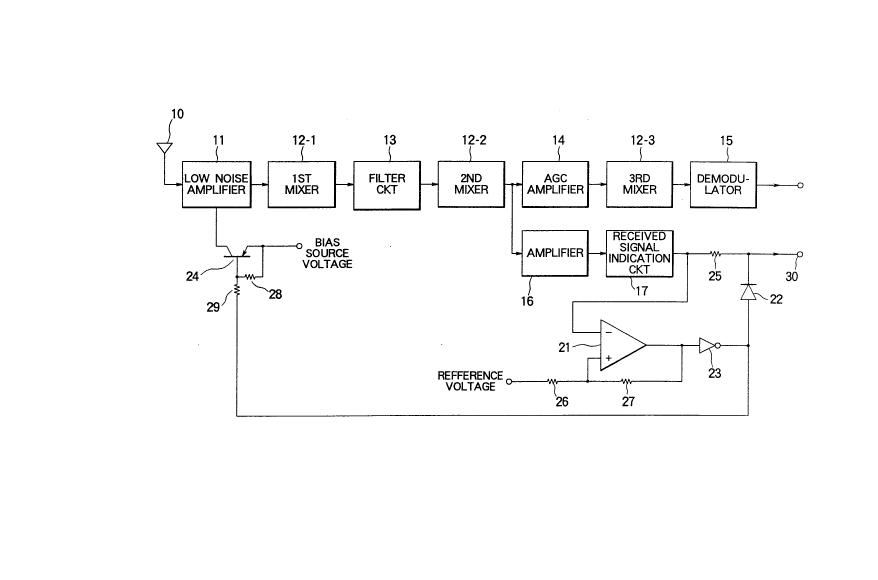
Referring to Fig. 1, a conventional receiver with
an AGC circuit will at first be described in order to
25 facilitate an understanding of this invention. The
receiver with an AGC circuit comprises a reception
antenna 10, a low noise amplifier 11 connected to the
reception antenna 10, a first mixer 12-1, a filter
~ :L~3~
circuit 13, a second mixer 12-2, an AGC amplifier 14, a
third mixer 12-3, a demodulator 15, an amplifier 16, and
an RSSI (Received Signal Strength Indicator) circuit 17.
An RF input signal is received through the
5 reception antenna 10, amplified by the low noise
amplifier 11, and converted by the first mixer 12-1 into
a first IF (Intermediate Frequency) signal. The first IF
signal is supplied to the filter circuit 13 through which
an undesired wave component in the first IF signal is
10 attenuated. The first IF signal is then converted by the
second mixer 12-2 into a second IF signal which is
supplied to the AGC amplifier 14. Supplied with the
second IF signal, the AGC amplifier 14 automatically
controls a gain to produce a gain controlled signal
15 having an average amplitude kept at a constant level.
The gain controlled signal is supplied to a third mixer
12-3. The third mixer 12-3 converts the gain controlled
signal into a baseband signal which is supplied to the
demodulator 15 as a demodulator input signal. The
20 demodulator 15 demodulates the demodulator input signal
into a demodulated digital data signal. When the average
amplitude of the demodulator input signal is not constant
and distortion is caused in the demodulator input signal,
the demodulated digital data signal inevitably contains
25 an error.
On the other hand, the second IF signal is also
supplied to the amplifier 16 and amplified into an
amplified signal. The amplified signal is supplied to
. ~ : :- .
2 ~
the RSSI circuit 17. The RSSI circuit 17 serves as a
detection circuit for detecting an input field strength
of the amplified signal. The RSSI circuit 17 produces a
strength indication signal indicative of the input field
5 strength as a voltage level. In the US digital cellular
system, the RSSI circuit 17 is required to report the
input field strength to a base station in the form of a
bit pattern as illustrated in Fig. 2.
Referring to Fig. 2, bit patterns "00000" through
10 "11111" represent input field strengths at every
predetermined interval (2dBm in Fig. 2).
Referring to Fig. 3, a characteristic
representative of the relationship between the input
field strength and an RF estimation strength must be
15 linearly varied within a range between -113dBm and
-51dBm.
In the above-mentioned conventional receiver with
an AGC circuit, however, the second mixer 12-2 and the
AGC amplifier 14 are saturated when the input field
20 strength is increased. This is because the low noise
amplifier 11 and the first mixer 12-1 have a high gain.
In this event, distortion is caused in the demodulator
input signal. As a consequence, the demodulator 15 can
not normally operate so that the demodulated digital data
25 signal inevitably contains an error.
Taking an economical efficiency into
consideration, the AGC amplifier 14 is allowed to have a
dynamic range of the order of 70dB at most. Thus, the
AGC amplifier 14 is normally operable at the input field
strength within a range between -115dBm and -45dBm. When
the input field strength is higher than -45dBm beyond the
above-mentioned range of the AGC amplifier 14, the
average amplitude is fluctuated. In order to avoid
fluctuation of the average amplitude, the second mixer
12-2 and the AGC amplifier 14 must have an increased
saturation level. The AGC amplifier 14 must have a wide
dynamic range. This results in a large-scale AGC circuit
and an increased amount of electric current supplied
thereto. It is therefore difficult to efficiently
realize a high saturation level and a wide dynamic range.
Referring to Fig. 4, description will now be made
as regards a preferred embodiment of this invention. In
Fig. 4, similar parts are designated by like reference
numerals and will not be described any longer. A
receiver with an AGC circuit according to this invention
comprises the circuitry illustrated in Fig. 1 and an
additional circuit connected between the low noise
amplifier 11 and an output side of the RSSI circuit 17.
The additional circuit comprises a comparator 21 having a
hysteresis characteristic, a diode 22, an inverter 23, a
switching transistor 24 connected to a bias voltage
source, a resistor 25 connected to the output side of the
RSSI circuit 17, resistors 26 and 27 connected to the
comparator 21, and resistors 28 and 29 connected to the
switching transistor 24.
- . ~ ::: . .
8 2 .1 ~
The additional circuit is divided into a first
circuit from the comparator 21 via the inverter 23 to the
switching transistor 24, and a second circuit from the
inverter 23 to the diode 22. The first circuit serves as
a bias control circuit for controlling supply of the bias
voltage to the low noise amplifier 11 by turning on and
off the switching transistor 24 to connect and disconnect
the bias voltage source. The second circuit serves as a
level output circuit for keeping the strength indication
signal, which is indicative of the input field stre~gth
as described in the foregoing, at a predetermined high
level while the bias voltage is not supplied to the low
noise amplifier 11.
Referring to Fig. 5 also, in the receiver with an
AGC circuit according to this invention, the output
voltage of the RSSI circuit 17, namely, the signal level
of the strength indication signal is varied with an
increase of the input field strength to exhibit a
characteristic depicted by a line A in the figure. The
comparator 21 has a first threshold level LH of a
predetermined high level and a second threshold level LL
(LH > LL) of a predetermined low level because of its
hysteresis characteristic.
In this embodiment, when the input field strength
is increased to -45dBm, the output voltage of the RSSI
circuit 17 increases to the first threshold level LH. In
this event, the comparator 21 produces a comparator
output signal having a low (logic zero) level. Supplied
2 ~ 3 ~ ~
with the comparator output signal having the low level,
the inverter 23 produces an inverter output signal having
a high (logic one) level to turn off the switching
transistor 24. In this event, the low noise amplifier 11
is not supplied with the bias voltage so that the low
noise amplifier 11 has an attenuation characteristic.
Thus, the input level is reduced by 30dB or so at the
first mixer 12-1 and at each of the subsequent circuit
components. Accordingly, the output voltage of the RSSI
circuit 17 exhibits a characteristic depicted by a line B
in Fig. 5. In other words, the output voltage of the
RSSI circuit 17 exhibits a characteristic which is
shifted from the line A to the line B when the output
voltage increasingly reaches the first threshold level
LH.
As far as the characteristic depicted by the line
A is followed, the AGC amplifier 14 is saturated when the
output voltage of the RSSI circuit 17 reaches the first
threshold level LH. However, transition from the line A
to the line B prevents the AGC amplifier 14 from being
saturated even if the input field strength is still
further increased by 30dB or so, as will readily be
understood from Fig. 5. Thus, by interrupting supply of
the bias voltage to the low noise amplifier 11 to make
the low noise amplifier 11 have the attenuation
characteristic, the dynamic range of the AGC amplifier 14
is expanded by 30dB or so. It is noted that the
characteristic of the line A is followed while the input
--:. :
2~ 1~3~1
field strength is between --115dBm and -45dBm.
Referring to Fig. 6, the output voltage of the
RSSI circuit 17, namely, the signal level of the strength
indication signal is decreased upon transition from the
line A to the line B. However, the inverter 23 then
produces the inverter output signal having a high level
which is applied through the diode 22 to provide an input
field strength indication signal. Thus, the input field
strength indication signal has a predetermined high
level. Therefore, such decrease of the output voltage of
the RSSI circuit 17 is never misunderstood as decrease of
the input field strength. To the contrary, the output
voltage of the RSSI circuit 17 is increased upon
transition from the line B to the line A as will later be
15 described in detail. However, the inverter output signal :
is then shifted from the high level to the low level so
that no high level output signal of the inverter 23 is
applied through the diode 22. Accordingly, the input
field strength indication signal is no longer derived
from the inverter output signal of a high level but now
corresponds to the output voltage of the RSSI circuit 17.
It is therefore possible to avoid misjudgement that the
input field strength is increased.
According to this invention, interruption of
supply of the bias voltage to the low noise amplifier 11
lowers the input level at each of the second mixer 12-2
and the AGC amplifier 14 by 30dB or so. Even if the
input field strength is further increased, the second
:: ~ . . .. ~ . . ~
2~1~3~
mixer 12-2 and the AGC amplifier 14 are never saturated
and the baseband signal produced from the third mixer
12-3 contains no distortion. It is assumed here that the
AGC amplifier 14 is normally operable at the input field
strength between -115dBm and -45dBm, namely, has an
inherent dynamic range between -115dBm and -45dBm.
According to this invention, the input level is lowered
by 30dB or so if the input level increases beyond -45dBm.
Accordingly, the dynamic range of the AGC amplifier 14 is
apparently expanded over a range between -115dBm and
-15dBm. As a consequence, the baseband signal produced
from the third mixer 12-3 has an average amplitude which
is kept constant at the input field strength up to
-15dBm. Accordingly, the demodulator 15 is supplied with
a demodulator input signal having a constant average
amplitude and no distortion even if the input field
strength is high. Thus, the demodulator 15 can normally
operate so that the demodulated digital data signal
contains no error.
Next, it is assumed that the input field strength
is decreased from the level higher than -45dBm down to
-50dBm. The output voltage of the RSSI circuit 17 is
decreased to the second threshold level LL of a
predetermined low level. In this event, the comparator
25 21 produces the comparator output signal of the high
level. As a consequence, the inverter 23 produces the
inverter output signal of the low level to turn on the
switching transistor 24. The bias voltage is then
3 ~ ~
12
supplied to the low noise amplifier 11 so that the
receiver with an AGC circuit carries out a normal
operation. Specifically, when the output voltage of the
RSSI circuit 17 is decreased to the second threshold
level LL, transition from the line B to the line A is
caused. As illustrated in Fig. 6, upon transition from
the line B to the line A, no high level output signal of
the inverter 23 is applied through the diode 22. Thus,
the output voltage of the RSSI circuit 17 is produced
. . .
straightforward as the input field strength indication
signal. It is therefore possible to avoid misjudgement .
that the input field strength is increased.
When the inverter output signal has the low
level, high impedance is observed from an output terminal
30 of the input field strength indication signal because
the diode 22 is connected to the inverter 23. This means
that the input field strength indication signal has no
influence of the inverter output signal having the low
level. As a result, the strength indication signal of
20 the RSSI circuit 17 is produced straightforward as the
input field strength indication signal. It is therefore
possible to correctly indicate the input field strength,
for example, within a range between -113dBm and -51dBm as
required in the US digital cellular system.
It is also possible to expand the dynamic range
of the receiver with an AGC circuit by addition of a
minimum circuitry and with no substantial increase of
electric current.
~. , ~ : : :
2 ~ 3 ~ ~
13
As described above, the receiver with an AGC
circuit according to this invention is normally operable
when the input field strength is low. When the input
field strength is increased, the low noise amplifier has
5 a reduced gain because the bias voltage is interrupted.
Accordingly, the dynamic range of the AGC amplifier is
expanded while each of the mixer and the AGC amplifier is
not saturated and produces the output signal free from
distortion. Consequently, the demodulator is normally
10 operable even if the input field strength is high. In
addition, when the bias voltage is not supplied to the
low noise amplifier, the input field strength indication
signal is kept at a high level corresponding to the high
input level. It is thus possible to avoid misjudgement
15 that the input field strength is decreased.