Note : Les descriptions sont présentées dans la langue officielle dans laquelle elles ont été soumises.
WO 93/04448 PG'f/GB92/00574
cony nascRrgn~Taort Arp~T~
FIELD ~F TH$ INVEHTIOId
This invention relates to coin discrimination apparatus
which has particular but not exclusive application to a
mufti-coin validator.
BAC~GIZO~ TO THE IriVENTI~i
In a conventional mufti-coin validator, coins pass
along a path past a number of spaced sensor coils which
are each energised to produce an inductive coupling
with the coin. The degree of interaction between the
coin and the coil is a function of the relative size of
the coin and coil, the material from which the coin is
made and also its surface characteristics. Thus, by
monitoring the change in impedance presented by each
coil, as the coin passes it, data indicative of the
coin under test can be provided. The data can be
compared with information stored in a memory to
determine coin denomination and authenticity.
._.~ . . ,. .
E
,.;.... .: '~. ..: -. -<, .. :; :~ .,.... .....: :.:., ;.~...- .:;' .....: >
... .. , ,, ,..,. , ,, .
. . . ... . .. .. . . : :.~~:.. ~ ,.....,. .,.. ~ . .. .. .. . . ,.r~.., .
....
WO 93/04448 PCT/GB92/00574
?1~~~~~
The geometry of the coils 3.n relation to the coin to be
tested, strongly influences the degree of interaction .
between the coin and the coil. By selecting different
coil geometries for the coil, different interactions
and hence different characteristics of the coin can be
tested.
For example, UR Patent No.. 2 169 429 in the name of
Coin Controls Limited discloses coin discrimination
apparatus utilising three inductive sensor coils, two
of which are disposed to one side of the coin path and
are of different diameters, together with a third coil
which is arranged to wrap around the path so that the
coin under test passes axially through it.
S~IRY t'aF ~ INVBNTI~1
The present invention provides an impx:oved way of
achieving an inductive coupling with a coin under
teat.
,
in accordance with the present invention there is
provided coin discrimination apparatus comprising: .
means for defining a path for coins under test, first
r.. . . ,~ ;,. ,,,
>,
..,
s. ,.3 4. . ~,
tv
~: t ~, .
s. :' t,..'";
~s'
1 v~~ .
4.
. .~,v.._ .S .. " ..... . ., ...." .. ..... , ... r , ..,.. ._arv ~, ~. , , .
, ,... .."..,.v , ,
WO 93/04448 PGT/GB92/00574
~~.i~ ~~~
- 3 -
and second inductor means for forming concurrent
inductive couplings with a coin under test during its
passage along the path, switching means for causing
energisation of the inductor means to produce a
sequence of coin tests wherein for each thereof a
different resultant inductive coupling is formed
between the inductor means and the coin depending upon
the manner of energisation of the first and second
inductor means, and sensor means for sensing said
resultant inductive coupling for each of said tests in
the sequence.
The inductor means conveniently comprise ffirst a~1
second coils disposed on opposite sides of the coin
path. The switching means conveniently is configured
to switch current in a bi-directional manner through
each of the first and second coils individually. The
sequence of tests performed on the coin under test may
comprise feeding current through the first coil
individually,.feeding current through the. second coil
individually, feeding current in the same sense through
both of said coils concurrently, and feeding current in
WO 93/04448 PCT/GB92/00574
~~~.:~a~~
opposite senses concurrently through said first and
second coils respectively. .
The sensing means may comprise means for sensing the
amplitude and/or frequency developed across the or each
said coil for each said test.
Conveniently, the coils are arranged in an oscillatory
circuit driven by an ac oscillator in a phase locked
loop which tends to maintain the frequency of the
oscillator at the natural resonant frequency of the
oscillatory circuit as the coin passes the coil. The
sensor means may comprise means for sensing the peak
amplitude deviation of the oscillatory signal during
each said test .
The peak amplitude deviations may be caapared in a
microprocessor with preprogramoned values in order to
determine coin authenticity and/or denomination.
An array of optical detecting means may be provided
adjacent the coin path for detecting coin diameter -
and/or thickness. .
::, ~. ~ :.
.. . . . .~.. ... .. . . . ,...... . ...... . . .~ . . s. ,.~:: .. . ~.:;: .
..
WO 93/04448 PG~'1GB92/00574
Z ~. ~. '~ ), r~ ~
- 5 -
BRIEF' DBSCRIPTIQN OF TBE DRrrWIBGS
In order that the inv~ntion may be more fully
understood an embodiment thereof will now be described
by way of example, with reference to the accompanying
drawings in whicha
Figure 1 is a schematic side elevational view of coin
discrimination apparatus according to the invention;
Figure 2 is an end view of the apparatus shown in
Figure 1;
Figures 3 to 6 are schematic flux diagrams for
different switching configurations of the sensor coils;
Figure 7 is a block diagram of electrical circuitry
asssociated with the apparatus; .
Figure ~ shows a signal representative of the results
of the sequential coin tests;
Figure 9 illustrates schematically an additional test
that can be perfomned with the sensor coils; and
WO 93/04448 PCT/GB92/00574
~'~.~~ )~~
-s-
Figure 10 is a block diagram of a modification to the
circuit of Figure 8, in which the coils are
additionally arranged to perfozm the coin diameter
test.
DES~IPTI0~1 O~F' EB~D
Referring to Figure 1, the apparatus consists of a body
1 including a coin inlet 2 in to which coins are
inserted from above so as to fall onto an anvil 3 and
then roll edgewise along a coin rundown path 4 past an
optical sensing station 5 and then past an inductive
sensing station 6. Outputs from the sensing stations
5, 6 are fed to electrical circuitry which will be
described hereinafter with reference to Figure 7, which
controls operation of an accept gate 7 shown in Figure
1. Thus, after leaving the inductive sensing station,
the coin falls towards the accept gate. If the gate 7
is opened, the coin will fall into a coin accept chute
8; otherwise, the coin is deflected by the gate 7 into
a reject chute 9.
::.,~. .
. ~: . ..
...... .... .~. .... ,......,.... . .., .. .. re ~.. v~o-S~ m .-..S.:v ,...,.
.. .... ...
WO 93/04448 PCT/GB92/OOS74
~1~.~ ~~~~
Referring to Figure 2, the body member 1 consists of
two hinged parts la, lb. The optical sensing station
consists of a linear array of light emitting devices
5a on the fixed side of the body, which are aligned
with a corresponding array of photodetectors 5b on the
hinged side of the body lb. The light emitting devices
and detectors are arranged in pairs so as to provide a
line of light rays extending transversely across the
coin rundown path 4. As the coin passes the optical
i0 sensing station 5, a number of the light rays are
interrupted in dependence upon the diameter of the
coin. Thus, by processing the outputs of the detectors
5b, a signal indicative of coin diameter can be
obtained. Furthermore, as explained in co-.pending GB
Application No. 9024988.9, the output signals from the
detectors 5b can be processed so as to compensate for
any variations in coin velocity or coin acceleration
down the rundown path 4. Also, by appropriately
modifying .the array of light mnitting devices and
20. detectors, it is also possible to obtain an indication
of coin thickness. Reference is directed to the
co-pending application aforesaid for a full description
of diameter and/or thickness measurement.
WO 93/04448 PGT/GB92/00574
_8_
The inductive sensing station 6 includes a pair of
inductor coils 6a, 6b arranged on opposite sides of the
coin rundown path, the coils having substantially
identical geometrical and electrical characteristics.
Each coil 6a, 6b is wound upon a plastic bobbin, with a
cylindrical ferrite shield 10a, lOb, arranged on a
common axis which extends normally of the major faces
of the coin as it passes between the coils 6a, 6b. A
coin 8 is shown schematically in dotted outline on the
coin rundown path 4 in Figure 1. The coils 6a, 6b are
selected to have a sufficiently sneill diameter and to
be located sufficiently close to the coin rundown path
that the inductive coupling produced between the coil
and the coin is virtually independent of the diameter
of coin user test and remains at a maximum value for a
portion of the time taken for a coin to pass the coils
6a, 6b. Typically, the coils have a diameter of 14 mm.
In accordance with the invention, a plurality of
inductive tests are performed on the coin 8 whilst it
passes through the inductive testing station 6. In the
present example, four inductive tests are performed as -
WO 93/04448 PCT/GB92/00574
~~~.!~~:~E?~
g
will be explained in more detail with reference to
Figures 3 to 6.
Test 110. 1
This test is carried out by energising coils 6a, 6b
with alternating currents in phase with each other so
that the coils produce electromagnetic fields that
constructively add to one another. The resulting flux
pattern is shown schematically in Figure 3 and is
referenced lla, ilb. It has been found that the
resulting inductive coupling between the coils 6 and
the coin 8 has a relationship in which the conductivity
of the coin is emphasised.
best l~Io. 2
.__ Referring to, Figure 4, in this test, the coils 6a, 6b
are energised in such a manner, i.e. in anti-phase, as
to° produce opposed electromagnetic fields. The
resulting flux pattern is shown sche~aatically in Figure
4 with flux equipotential lines being referenced llc,
d, e, f. It has been found that the inductive coupling
betr~een the coils 6a, 6b and the coin 8 has a
WO 93/04448 PCT/GB92/00574
?~~.~~2~
-lo-
relationship in which the permeability of the material
from which the coin 8 is made, is emphasised.
Test No. 3
Referring to Figure 5, in this test, coil 6a is
energised individually i.e, without coil 6b being
energised. The resulting flux pattern is shown by
equipotential lines lig, h. It has been found that the
inductive coupling between the coin 8 and coil 6a has a
relationship which is strongly influenced by the facial
indentation of the coin 8.
Test Ido. 4
Referring to Figure 6, in this test, coil 6b is
energised individually i.e. without energising coil 6a.
The resulting flux pattern is shown by eguipotential
lines lij, k: For this test, the inductive coupling
between the coil 6b and coin 8 is strongly influenced
by coin thickness.
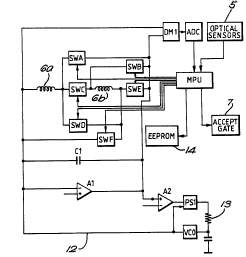
Referring to Figure 7, strive current for performing the
four tests is fed through the coils 6a, 6b under the
WO 93/04448 PGT/GB92/00574
2~.~.~a~~
- 11 -
control of transistor switches SWA, B, C, D, E, F
operated by a microprocessor MPU.
The coils 6a, 6b are connected in an oscillatory
circuit which includes the capacitor C1. The
oscillatory circuit has its own natural resonant
frequency when no coins are in the proximity to the
coils 6a, 6b. The circuit is driven by a ghase locked
loop at its natural resonant frequency by means of a
voltage controlled oscillator VCO which produces an
oscillatory drive signal on line 12. The resonant
circuit 6a, 6b, C1 is connected in a feedback path to
an op~rational amplifier A1, the output of which is
inverted by amplifier A2 and the resulting signal is
compared in phase comparator PS1 with the output of the
voltage controlled oscillator VCO on line 12. The
output of the phase cator PS1 comprises a° control
voltage on lime 13 which is used to control the
frequency of the voltage controlled oscillator VCO.
The phase locked loop maintains 180° phase difference
across the amplifier A1, which is the required
condition to maintain the oscillatory circuit 6, C1 at
. its natural resonant frequency.
a
,, .. ..~ -.
r .x
. .r~: .. _ , . _ ._; "~. _ . .: . . ~. ~. ,-. : :..~ . <. ..... . :,: . . ~ -
' , -'_ .. :v..; .
WO 93/04448 PCT/GB92/00574
- 12 -
In the absence of a coin, the apparatus operates in an
idle mode, in which the microprocessor MPU, the analog
to digital converter ADC, the demodulator DM1 and the
phase locked loop remain substantially inactive. A
wake up sensor (not shown) which may comprise a sample
optical detector, detects the presence of a coin on the
rundown path 4 and produces a signal which causes the
apparatus to switch from the idle mode to an active
mode. L~nediately after the apparatus becomes active
but before the coin reaches the sensing station 6, the
microprocessor MPU switches the switches SWA-F in a
sequence such as to feed current sequentially through
the coil 6a, 6b in a manner to perform the
aforementioned tests 1 to 4. Thus, the switches are
operated in accordance with the sequence eet out in
Table 1.
Table 1
S,ritch SWA SwB SWiC SWD Si~IE SwF'
Test 1 0 0 1 0 1 0
Test 2 0 1 0 1 0 0
Test 3 1 0 0 0 0 0
Test 4 0 1 0 0 0 1
.... , n.:~,.. ,:.:j: ;...,~.:;. : .'.,,:'~w.;... .:.w.,,.. '.. .,,.s. .,. i:
y..... ,,'...:, - :-~:;.
f
~7 7 a : t~... .~
.v,
1 ", A
i,.. :'. . .. '.:':' .. ~~~ ~.. .. , '~ . ,"... ."; .,, v,_j ,,,,'.;,..~ .o~
,. :,~. . ;,;'..; , ,'.'-~. , t.......,'.:.. . ' ~.., '..,.;
WO 93/04448 PCT/GB92/00574
- 13 -
In the Table, logic level 1 indicates a conductive
switching state whereas logic level 0 represents a non-
conductive switching state.
As the aforementioned Tests Nos. 1 to 4 are performed,
a demodulator DM1 produces a signal representative of
the amplitude of the oscillation developed for each
test. Each of the four amplitudes is digitised by an
analog to digital converter ADC and then stored by the
microprocessor BpU to provide base reference values.
For each test condition, the voltage controlled
oscillator VCO will be driven at a frequency to
maintain the resonant circuit at its natural resonant
frequency for the test concerned.
Referring to Figure 8, once the base reference values
have been established, the microprocessor RPU operates
the switches SWA-F in order to perfornn one of the four
tests, for example Test No. 1. The apparatus remains
in this configuration until the microprocessor MPU
detects a plateau in the amplitude of the oscillation
developed during the test, indicated at A, or a
predetermined time has elapsed, in which case the
WO 93/04448 PCT/GB92/00574
Z~~~~~~
- 14 -
apparatus returns to its idle mode. The detection of
the plateau indicates that the coin is at the testing
station G and that, due to the arrangement of the coils
6a, 6b, the coupling will remain at a maximum for the
duration of each of the tests Nos. 1 to 4. This means
that although the output from the demodulator DM1
varies between tests, it remains substantially
constant during each test.
If the plateau is detected, the microprocessor MPU
stores the output from the analog to digital converter
l,DC and proceeds to operate the switches SWA-F in order
to perform sequentially the remaining tests, the
results of which are also stored.
-
I For each test, the phase locked loop operates to
maintain the circuit in resonance: In.the presence of
the coin, the inductive coupling between the coils 6a
or 6b alters the natural resonant frequency of the
resonant circuit defined by coil 6 in the capacitor C1:,
the inductive coupling being a function of
characteristics of a coin. As previously discussed,
each of the four test results in an inductive coupling
WO 93/04448 PCT/GB92/00574
- 15 -
in which a particular characteristic of the coin is
emphasis~d. During each of the four sequential tests,
the voltage controlled oscillator VC~ maintains the
resonant circuit 6, C1 at its natural resonant
frequency, this frequene:y having been altered as a
result of the inductive coupling between the coils and
the coin. This results in a substantial amplitude
variation in signal level being produced across the
resonant circuit in comparison to that produced
immediately after wake up. The amplitude variation is
detected by demodulator DM1, an example of the
output of which is shown in Figure ~, and digitised by
the converter ADC. The amplitude, in the presence of
a coin for each test is then compared by the
microprocessor with the aforementioned base reference
values in order to provide a peak amplitude deviation
for each of the four tests. These peak amplitude
deviations are compared with stored values indicative
of reference coins preprogranmred in an EEPROM 14
connected to the microprocessor MPV.
WO 93/44448 PCT/GB92/00574
- 16 -
Also, the microprocessor 1~U receives signals from the
optical sensors 5 and processes them in order to obtain
coin diameter information in the manner described in
co-pending GB application 9024988.9 aforesaid. The
diameter information is also compared with preprogramed
values held in the EEPROM 14 for reference coins.
Thus, in this way, data representative of the coin
under test can be compared with preprogranmied values
in the EEPROM 14 in order to determine coin
authenticity and denomination. If the coin is found to
be acceptable, an enable signal is sent to accept gate
7 in order to allow the coin to pass into accept chute
8 (Figure 1).
.. From the foregoing, it will be appreciated that the
deonodulator DM1 operates as a sensor means for sensing
the inductive coupling between the coils 6a and/or 6b
during the sequence of the four tests, the inductive
coupling being manifested as an amplitude.variation as
a result of the phase locked loop holding the resonant
circuit at its natural resonant frequency in the
presence of a coin. The advantage of using such a phase
-,. :. ..;. . ... ,.,..... ,~_,...... . .. ,..,.: _ ,.,~; ,. ':.:v:~ .m, ,
:'::~, ,.., . ;' ~. ., .. . l 1 :s-;..' ~~:..y:. ,. ::'.,. , , ,.~,~,.
;A,.~~.. ~. . . ,.,.... ,_
w
,f. : . _ ,. - ~: . , .,_ . ~." , ,... '.s:.. ."" . , :'.:'a ~. ~..~.,', ~ .1~
:.~.:. ~, :i.': [ v1'... ' ": , ':. . '.L.. ,, _ . ,.
WO 93/04448 PGT/GB92/00574
- 17 -
locked loop arrangement is discussed in detail in GB
Patent Specification 2 169 429. However, the
inductive coupling can also be manifested in terms of a
frequency change in which case the sensor means may
sense a frequency deviation across the resonant circuit
6, C1.
Referring now to Figures 9 and 10, a modification will
now be described in which the coils 6a, 6b are
connected in such a way as to provide coin diameter
information by the performance of additional tests on
the coin. This enables the optical sensing station 5
to be dispensed with, thereby simplifying the
construction of the apparatus. To this end, the coils
6a, 6b are made larger than described with reference to
Figures 1 to 7 and/or are mounted in a higher position
relative to the coin rundown path, so that the
~ductive coupling between the coils is influenced by
coin diameter.
best 1~. 5
The general principle of the test referred to herein as
Test 5, will be described. For this test, the coils
WO 93/04448 PCT/GB92/00574
~~~.~5~~
-is-
are connected to provide a transmit-receive
arrange~nt. As shown in Figure 9, the coil 6b is used
as a transmitter and the coil 6a is used as a receiver.
As previously explained, for Tests Nos. 1 to 4, the
self inductance of the coil 6a and/or 6b is monitored
and the relatively small size of the coil relative to
the coin produces a signal which, in the presence of a
coin, is substantially independent of the coin
diameter. However, it has been found for Test No. 5
that when the coin passes the coil arrangement, the
leakage of flux around the coin into the receiver coil
6a is a function of the coin diameter. Thus, by
measuring the amplitude of the signal induced in the
receiver coil 6a, a signal as a function of coin
diameter is provided.
Figure 10~ illustrates how the circuit of Figure 7 can
be modified in order to perform Test No. 5. Additional
switches SWG - J are provided, connected as shown.
Test Nos. 1 -, 5 are performed by operating the
switches according to the following table.
WO 93/04448 PGT/~GB92/0057a
- 19 -
Table 2
Switch SWA SWB SWC SWD SWE SWF, SWAG SW8 SWI SWJ
Test 1 0 0 1 0 1 0 0 1 1 0
Test 2 0 1 0 Z 0 0 0 1 1 0
Test 3 Z 0 0 0 0 0 0 1 1 0
Test ~ 0 1 0 0 0 1 0 1 1 0
Test 5 0 1 0 0 0 1 1 0 0 1
In the Table, logic level 1 indicates a conductive
switching state whereas logic level 0 represents non-
conductive switching state.
During the performance of Test No. 5, the transmitter
coil 6b is connected in an oscillating circuit
including amplifier A1 and capacitor C1 as previously
described with reference to Figure 7. The receiver
coil 6a however, is connected through switches SWiG and
SWJ in parallel with capacitor C2 and the output of the
resulting resonant circuit is fed through amplifier A3
and isolating capacitor C3 to the input of the
demodulator DM1. In this arrangement, the amplitude of
the signal induced in coil 6a is a function of coin
diameter and is detected by demodulator DM1 for
WO 93/04448 PGT/GB92/00574
z~~.~ ~1~
- 20 -
comparison with preprogrannned values in the
microprocessor MPU.
It will be appreciated that by providing appropriate
switches, it will be possible to perform an additional
test, Teat 6 in which the coil 6a is used as a
transmitter and coil 6b is arranged as the receiver.
This configuration may be used to cross check against
the result of Test 5.
As a modification, separate coils may be provided for
carrying out Test 5 and/or Test 6, the segarate coils
being switched by respective switches (not shown) under
the control of the ta3.croprocessor 1~U. Thus, Tests 1-4
Would be performed with coils 6a, 6b as described with
reference to Figures 1 to 8, and thereafter, as part of
the test sequence, the separate coils would be
energised to perform Test 5 and/or Test 6..
It would be possible to measure diameter by means of a
separate inductive coil arrangement in which case the
test results would be affected by diameter as well as
r.
,S -.
t
r. ,5 ; -.
..t .. a' .~ . p. ,
,v:
, . , . t-'. ,.. . . . . .
a.a . . .. . ~ . .. .~ ~ , .,... , .. .... . .. ".1,~... ... ,..4.,~,~, , ~,
1. .. , , .. .
WO 93/04448 FCT/GB92/005'~4
- 21 -
thickness, metal content and surface characteristics of
the coin under test.