Note : Les descriptions sont présentées dans la langue officielle dans laquelle elles ont été soumises.
PERIODIC DOM~IN REVER8AL EI.ECTRO-OPTIC MODULATOR
BACKGROUND OF THE INVENTION
1. Technical Field
This invention relates generally to electro-optic
modulators for modulating optical signals and, more
particularly, to a phase velocity matched electro-optic
modulator.
2. Discussion
Travelling wave integrated electro-optic
modulators are known in the art for providing amplitude
and phase modulation of an optical signal. Electro-optic
modulators are commonly used with fiber optic links which
have become increasingly important for a number of
applications that include millimeter wave communications
and radar systems. An external electro-optic modulator is
generally required for a millimeter wave fiber optic link
since direct modulation of a solid state laser signal
generally is not possible above microwave frequencies.
Electro-optic modulators typically include an
optical waveguide formed in a substrate and having an
overlying metallic electrode structure. Electro-optic
modulators fabricated in substrate materials in which the
optical and microwave phase velocities are equal offer the
potential of very broad modulation bandwidths. However,
for important electro-optic substrate materials such as
lithium niobate (LiNbO3), there is an inherent mismatch
between the optical and RF microwave velocities. Since
the optical signal phase velocity in lithium niobate is
nearly twice the microwave drive signal velocity, the
magnitude of the phase modulation begins to degrade as the
phase difference between the optical and drive signals
increases. This phenomenon is often referred to as phase
"walk off".
This velocity mismatch necessitates design trade-
offs. On the one hand, the maximum achievable drive
frequency decreases as the modulator length is increased.
on the other hand, to lower the drive voltage and power
that is required, a longer device length is generally
required. Thus, a trade-off is generally made between
maximum drive frequency and required drive power.
Prior attempts have been made in order to
compensate for the inherent velocity mismatch. Periodic
electrode structures have been used in coplanar electro-
optic modulators and are generally categorized as periodic
phase reversal electrodes or intermittent interaction
electrodes. Known periodic electrode configurations
include unbalanced transmission lines which are asymmetric
about a propagation axis. However, this may lead to
incompatibility with the balanced line transitions to
other fiber optic link transmitter components.
A more recent example of an electro-optic
modulator is found in U.S. Patent No. 5,005,932 issued to
Schaffner, et al. This prior art modulator achieves
velocity matching of the optical and RF signal by
employing travelling wave electrodes with periodic
discontinuities. While this approach is generally
feasible for most applications, the discontinuities may
inherently cause reflection of portions of the RF signal
back toward the source along with electromagnetic
scattering of portions of the RF signal into the lithium
niobate substrate. As a consequence, such prior art
approaches generally suffer from these losses, especially
at high frequencies such as those in the millimeter wave
range.
It is therefore desirable to provide for an
improved electro-optic modulator which does not suffer
from undesirable RF reflections or scattering such as
that which may be present in the prior art. In
particular, it is desirable to provide for an improved
technique of resetting the phase difference in millimeter
wave integrated electro-optic modulators which exhibit
velocity mismatches between the RF and optical signals.
SUMMARY OF THE INVENTION
In accordance with the teachings of the present
invention, an electro-optic modulator is provided which
compensates for phase velocity mismatch between an
optical signal and an RF signal. The modulator includes
an optical waveguide formed in a ferroelectric substrate
and coupled to an optical input. An RF waveguide is
formed on the substrate for applying an electric field to
a region adjacent to the optical waveguide so as to
modulate an optical signal. The ferroelectric substrate
has domain regions which compensate for phase differences
within the modulation region. In a preferred embodiment,
the RF waveguide couples to an optical waveguide Mach-
Zehnder interferometer to provide for amplitude
modulation (AM) of the optical signal.
Various aspects of the invention are as
follows:
An electro-optic modulator comprising:
a substrate having a ferroelectric domain;
optical waveguide means formed in said
substrate penetrating at least one opposite change in
direction in said ferroelectric domain;
optical input means for coupling an optical
input signal to the optical waveguide means;
., ' 1
..
3A
RF waveguide means formed on said substrate and
applying an electric field to a region overlying the
S optical waveguide means to thereby induce modulation of
said optical signal;
electric drive source means for coupling an RF
electric signal to the RF waveguide means;
periodically inverted and non-inverted regions
which compensate for phase differences within said
modulation; and
optical output means for providing a modulated
optical output signal.
An electro-optic modulator comprising:
a substrate having a ferroelectric domain;
an optical waveguide having at least two
generally parallel optical waveguide channels formed in
said substrate;
an RF waveguide formed on said substrate and
having a modulator active region overlying the optical
waveguide channels;
optical input means for coupling an optical
signal of a given phase to the optical waveguide;
electromagnetic drive source means for coupling
electromagnetic energy to the RF waveguide;
periodically inverted and non-inverted regions
for changing the direction of the electric field at
locations where said optical signal and said RF signal
are substantially 180 degrees out of phase; and
optical output means for providing an amplitude
modulated optical output signal.
A method for modulating an optical signal
comprising:
supplying an optical input signal to an optical
waveguide that is fabricated in a substrate, said
substrate comprising a polymer;
. .,~
,j .
$ ~ ~
3B
splitting said optical input signal between
first and second optical waveguide channels;
S generating an electric signal across said
optical waveguide within an active modulation region so
as to induce phase modulation;
applying said optical input signal through said
optical waveguide via inverted and non-inverted regions
of a ferroelectric domain found within said active
modulation region;
and combining said phase modulated optical
signals from each of said first and second optical
waveguide channels to provide a modulated output signal.
A method for modulating an optical signal
comprlslng:
supplying an optical input signal to an optical
waveguide that is fabricated in a substrate comprising a
polymer;
generating an electric signal across said
optical waveguide within an active modulation region so
as to induce phase modulation;
applying said optical input signal through said
optical waveguide via inverted and non-inverted regions
of a ferroelectric domain found within said active
modulation region; and
supplying a modulated output signal.
BRIEF DESCRIPTION OF THE DRAWINGS
Other objects and advantages of the present
invention will become apparent to those skilled in the
art upon reading the following detailed description and
upon reference to the drawings in which:
FIG. 1 is a top view of a conventional periodic
phase reversal electro-optic modulator in accordance with
the prior art;
4 ,~ ~ ~ 4 ~ ~ ~
FIG. 2 is a top view of an electro-optic
modulator in accordance with the preferred embodiment of
the present invention;
FIG. 3 is a cross-sectional view taken along line
3-3 of FIG. 2;
FIG. 4 is a graphic display which illustrates the
frequency response for one example of an electro-optic
modulator in accordance with the present invention;
FIG. 5 is a top view of an electro-optic
modulator in accordance with an alternate embodiment of
the present invention; and
FIG. 6 is a cross-sectional view taken along
lines 6-6 of FIG. 5.
lS DETAILED DESCRIPTION OF THE PREFERRED EMBODIMENTS
An existing electro-optic modulator 10 is
provided in FIG. 1 in accordance with the prior art. The
prior art electro-optic modulator 10 shown herein is a
periodic phase reversal (PPR) modulator which is
fabricated on a lithium niobate (LiNbO3) substrate 12. The
prior art PPR modulator 10 incorporates an integrated
optic Mach-Zehnder interferometer for transmitting an
optical signal therethrough and a periodic phase reversal
(PPR) electrode for applying an electric field to the
optical signal to induce phase modulation thereon.
According to the prior art, the Mach-Zehnder
interferometer includes a pair of optical waveguide
channels 16 and 18 formed in the substrate 12 which have
portions thereof located parallel to one another. The
interferometer further includes an optical input path 14
that leads to an input Y-junction 15 which in turn splits
an optical input signal 13 between the first and second
optical waveguides 16 and 18. The interferometer likewise
includes an output Y-junction 27 which joins the output of
the first and second optical waveguides 16 and 18 and
provides an amplitude modulated (AM) output signal 29 to
a modulator output path 28.
The PPR electrode includes an active center
conductor 22 and a pair of grounded conductors 24a and 24b
S which apply an RF electrical field across the optical
signal 13. The center conductor 22 is disposed above an
area between optical waveguides 16 and 18. The pair of
grounded conductors 24a and 24b are disposed above an area
on the outer sides of optical waveguides 16 and 18.
Accordingly, the center conductor 22 receives the RF
signal from a power source 23, while the grounded
conductors 24a and 24b are generally coupled to the low
ground reference.
Accordingly, the optical input signal 13 travels
through the optical waveguides 16 and 18 and interacts
with the RF input signal 25 so as to generate phase
modulation thereon. However, it is generally known that
the phase velocity of an RF electric signal is generally
less than the phase velocity of an optical signal by
approximately a factor of 0.6 in lithium niobate. Thus,
if the modulator 10 is long enough, the phase difference
between the RF signal and the modulation induced on the
optical signal will reach 180 degrees at some point. In
order to compensate for this phase difference, the
conventional approach uses the periodic phase reversal
electrode to reverse the direction of the electrical field
with respect to the optical signal by jogging portions 20
of the electrode around the optical waveguides 16 and 18.
The effect of this is to make the total phase difference
between the modulation on the optical signal 13 and RF
signal 25 become 360 degrees and to thereby realign the RF
and optical signals.
Accordingly, the prior art approach provides for
an electrode having air gaps 21 with electrode jogs 20 at
locations in which the phase difference between the RF
electric signal 13 and the modulation on optical signal 25
reaches a 180 degree difference. However, the prior art
approach requires that the RF signal 25 be physically
moved about the sides of the optical waveguides 16 and 18
by periodic electrode discontinuities. At very high
frequencies, the prior art discontinuities generally cause
a fraction of the RF signal 25 to be reflected back toward
the RF source 23 and a fraction of the RF signal 25 to be
scattered into the substrate 12. As a consequence, this
back-reflection and scattering results in undesirable
signal loss.
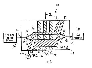
Turning now to FIGS. 2 and 3, a periodic domain
reversal electro-optic modulator 30 is shown therein in
accordance with the present invention. The periodic
domain inversion electro-optic modulator 30 is fabricated
on the +Z face of a lithium niobate (LiNbO3) substrate 32
in accordance with a preferred embodiment of the present
invention. The substrate has a ferroelectric domain with
selected regions formed to provide opposite changes in
direction. The modulator 30 includes an integrated optic
Mach-Zehnder interferometer for guiding an optical signal
56 through the modulator 30. The modulator 30 further
includes an asymmetric coplanar waveguide travelling wave
electrode for applying an electric field across the
optical signal 56 to induce phase modulation on the
optical signal 56 in each waveguide.
The interferometer includes an optical input
terminal 34 for receiving an optical input signal 56 and
an output terminal 44 for providing an amplitude modulated
~AM) optical output signal 60. The interferometer further
includes an input Y-junction 36 which splits the optical
input signal 56 between a pair of optical waveguide
channels 38 and 40. The pair of optical waveguide
channels 38 and 40 have portions thereof that are located
substantially parallel to each other. The interferometer
likewise has an output Y-junction 42 which combines the
pair of optical waveguide channels 38 and 40 which in turn
then leads to the output terminal 44.
The interferometer and associated optical
waveguide channels 38 and 40 are fabricated within the
lithium niobate substrate 32 by diffusing titanium into
the substrate 32 to form the optical waveguide channels 38
and 40 in accordance with established techniques known in
the art. The optical waveguide channels 38 and 40 are
formed with portions arranged substantially parallel to
one another which are subjected to one or more opposite
changes in direction in the ferroelectric domain. In
addition, a silicon dioxide buffer layer 62 is preferably
disposed on top of the substrate 32 for purposes of
preventing optical losses from the optical waveguide
lS channels 38 and 40 that may otherwise be caused by the
metallic electrodes 46 and 48.
The asymmetric coplanar waveguide travelling
wave electrode is formed on top of the buffer layer 62 in
an area substantially above the first and second waveguide
channels 38 and 40. The travelling wave electrode
includes an active conductive line 46 and a conductive
ground line 48. The active conductive line 46 is coupled
to an RF power source 58 for receiving the RF electric
signal 59. The conductive ground line 48, on the other
hand, is coupled to ground. The active conductive line 46
is displaced from the conductive ground line 48 and, as a
result, forms an active modulation region 50 and operates
to apply an RF electric field across the modulation region
50. Accordingly, the electric field causes the optical
inp~t signal 56 to be phase modulated in each of the
optical waveguide channels 38 and 40.
According to the present invention, the
modulator 30 is fabricated in a substrate 32 which has a
ferroelectric domain that has inverted regions 54 and non-
inverted regions 52. The inverted and non-inverted
regions 54 and 52 of the ferroelectric domain are defined
during the fabrication process through photolithographic
techniques known in the art. One such technique is
described in an article by Shintaro Miyazawa, entitled
"Ferroelectric Domain Inversion in Ti-Diffused LiNbO3
Optical Waveguide", J. Appl. Phys., 50(7), July 1979, pgs.
4599-4603. In so doing, a thin titanium layer of
approximately 500 angstroms is evaporated within each of
the regions that are to be formed into inverted regions
52. The titanium is then diffused into the substrate 32
at a temperature above the Curie temperature for titanium
doped lithium niobate at approximately 1000 degrees
Centigrade, so that the ferroelectric domain inversion may
occur.
The inverted and non-inverted regions 52 and 54
are selected so as to provide phase compensation at
locations selected along the optical waveguide channels 38
and 40 where the phase difference between the modulation
of optical input signal 56 and the RF electric signal 59
reaches 180 degrees. Accordingly, this compensation
changes the sign of the induced phase modulation of the
optical signal 56 so that the overall phase difference
between the modulation of optical signal 56 and RF
electric signal 59 is 360 degrees and the signals are back
in phase. This enables the modulator 30 to achieve
continued modulation gain.
In operation, the periodic domain reversal
electro-optic modulator 30 receives an optical input
signal 56 which passes through the optical waveguide
channels 38 and 40. The RF electric signal 59 is applied
via an RF power source 58 to generate an electric field
which in turn induces phase modulation on optical input
signal 56. In doing so, the optical input signal 56 is
received by an input terminal 34 which leads to an input
Y-junction 36 that evenly splits the optical input signal
56 between first and second optical waveguide channels 38
and 40.
g
Optical waveguide channels 38 and 40 have
portions which extends substantially parallel to one
another and subject the optical input signal 56 to the
electric field within active modulation region 50. As the
optical signal 56 passes through each of optical waveguide
channels 38 and 40, the optical signal 56 in each channel
is phase modulated. In doing so, the optical signal 56
passes through inverted regions 54 and non-inverted
regions 52 of the ferroelectric domain within the active
modulation region 50. Each transition between inverted
region 54 and non-inverted regions 52 changes the sign of
the induced phase modulation of the optical signal. This
compensates for 180 degree phase difference between the
modulation on optical signal 56 and the RF electric signal
59 caused by the phase velocity mismatch between the RF
and optical signals.
The optical waveguides 38 and 40 are joined
together at an output Y-junction 42 which leads to an
output terminal 44. Accordingly, the phase modulated
optical signals are brought together and combined via the
output Y-connector 42 so as to achieve an amplitude
modulated (AM) output signal 60. The principle of
combining the pair of phase modulated optical signals to
form an amplitude modulated signal is well known in the
art and therefore need not be explained herein. It is
conceivable that if one desires a phase modulated output
signal, a single optical waveguide could be employed in
place of the first and second optical waveguides 38 and 40
without departing from the spirit of this invention.
In accordance with one example of the preferred
embodiment of the present invention, calculated
performance data is provided in a graph showing relative
optical modulation 64 over a normalized frequency range in
FIG. 4. The particular example used therein provided for
an active modulation region 50 in which the optical input
signal 56 is subjected to seven periodic inverted and
non-inverted regions 52 and 54 at a frequency of
approximately 60 GHz. This means the modulator 30
provided for phase compensation a total of six times.
Accordingly, the graph shows very high performance for
amplitude modulating an optical signal with minimal loss.
According to FIG. 4, the frequency is normalized
to the design frequency of sixty (60) GHz and the optical
modulation 64 is normalized to the peak response. The
periodic domain reversal modulator 30 has a bandpass
because at normalized frequencies away from 1.0 the phase
modulation of the optical signal is changed by 180 degrees
at the inverted/non-inverted domain boundaries, but the
phase difference between the optical and RF signal is not
180 degrees at the boundaries. Thus, a residual phase-
mismatch exists at the beginning of each modulationsection and the accumulation of this residual phase-
mismatch causes the degradation of the modulator response.
With particular reference to FIGS. 5 and 6, an
alternate embodiment of the periodic domain reversal
electro-optic modulator is shown therein in accordance
with an alternate embodiment of the present invention.
The alternate embodiment of the electro-optic modulator 70
is fabricated with an electro-optic polymer 78 which may
include an organic polymeric nonlinear optical material
such as 4-dimethylamino 4'-nitrostilbene (DANS). A
conductive ground plane 74 is disposed on the silicon
substrate material 94 to form a microstrip RF transmission
line. A cladding layer 76 is disposed on top of the
conductive ground plane 74 and has a thickness of
approximately four (4) microns. An electro-optic polymer
layer 78 is disposed on top of the cladding layer 76 and
has a preferred thickness of approximately two (2)
microns. A second cladding layer 80 is further disposed
on top of the electro-optic polymer layer 78.
The electro-optic polymer layer 78 contains a
pair of optical waveguide channels 32' and 40' which are
formed in accordance with photo bleaching techniques known
in the art. One such photo bleaching technique is
described in an article by D.G. Girton, et al~, entitled
"20 GHz Electro-Optic Polymer Mach-Zehnder Modulator",
Appl. Phys. Lett. 58 (16), April 22, 1991, pgs. 1730-32.
Inverted and non-inverted regions 86 and 88 are formed in
optical waveguide channels 38' and 40' by polling the
electro-optic polymer 78 with an electric field so as to
align the ferroelectric domains accordingly. A pair of
active conductive lines 90 and 92 are formed on top of the
second cladding layer 80 for inducing an electromagnetic
field from each of the conductive lines 90 and 92 to the
ground conductive plane 74. As a consequence, the electric
field passes directly through each of the optical
waveguide channels 38' and 40' to provide phase modulation
thereto.
In view of the foregoing, it can be appreciated
that the present invention enables the user to achieve an
enhanced electro-optic modulator (30 or 70) which
compensates for phase velocity mismatches. Thus, while
this invention has been disclosed herein in combination
with particular examples thereof, no limitation is
intended thereby except as defined in the following
claims. This is because a skilled practitioner recognizes
that other applications can be made without departing from
the spirit of this invention after studying the
specification and drawings.