Note : Les descriptions sont présentées dans la langue officielle dans laquelle elles ont été soumises.
W093/0~98 ~ 1 1 5 1 ~ 2 PCT/US9l/~9l8
DescriPtion
Electrophoretic DisPlay Panel With
Selective Line Erasure
Technical Field
This invention relates to electro-optical
display devices in general, and more particularly, to
a display panel employing the electrophoretic effect
for producing a display image.
Background Art
The electrophoretic effect is well known and
many display devices have been designed using the
electrophoretic effect to produce graphic images. One
type of conventional electrophoretic display panel is
shown in U.S. Patents 4,655,897 and 4,742,345, which
are commonly owned by the assignee of the present
application. The electrophoretic display panel has
grid and cathode conductors spaced from an anode
conductor with an electrophoretic dispersion in
between them. Particles of a dielectric pigment
material having a light color are uniformly dispersed
in a dark-colored non-conductive suspension medium.
The particles in different pixel areas of the display
can be made to migrate towards the anode by
selectively biasing the cathode negatively with
respect to the anode. The migration of the particles
from the cathode to the anode, or vice versa, is used
to form an image by a change in contrast of the light-
colored particles against a dark-colored background of
the medium.
An electrophoretic display of the above-
described type has many advantages in that the
materials used are relatively inexpensive, while the
image formed can be maintained even when the power is
W093/0~98 PCT/US91/05918
2115152 -2-
removed. In order to erase the image, the cathode is
biased positively with respect to the anode, i.e. to
create an electric field of the opposite polarity.
In the prior art electrophoretic display
devices, the anode is a unitary planar structure to
which one voltage is applied in the write mode and a
different voltage is applied in the erase mode. All
lines of the displayed image are erased simultaneously
upon application of the erase voltage to the anode,
and all lines of the display must be rewritten to form
the next image frame. The next frame may often have
character lines or image portions which are the same
as the previous frame. Because all lines are
rewritten each time a new frame is displayed, the
process of displaying a new frame is slowed
accordingly.
It is therefore an object of the invention
to provide an electrophoretic display which overcomes
the aforementioned disadvantage of conventional
devices. In particular, the object of the invention
is to provide an electrophoretic display in which one
or more lines of the display can be selectively erased
and rewritten without disturbing the other image lines
which remain the same from one frame to the next. It
is a further object to provide a simple and
inexpensive circuitry for enabling such selective line
erasure in an electrophoretic display.
Disclosure of the Invention
In accordance with the invention, an
electrophoretic display apparatus comprises a panel
having a display surface and containing an
electrophoretic dispersion of particles in a
suspension medium, writing means for forming an image
on the display surface in a write mode by attracting
- 3 -
charged particles from the dispersion onto the display surface
in a plurality of image lines, and line erasing means for
selectively erasing an image line in a line erase mode by
repelling charged particles from only a portion of the display
surface corresponding to the image line to be erased.
In the preferred form of the invention, the display
surface is the cathode of the electrophoretic display, and the
line erasing means comprising a multiplicity of anode line
segments and line control means for individually controlling
the potential applied to each anode line segment. For
primarily a text display, each anode line segment is a
longitudinal rectangular conductor having a height
corresponding to the height of a text character line. The
line control means comprises a corresponding multiplicity of
switch elements for switching the potential applied to an
anode line segment to be erased from a first potential for
writing to a second, different potential for erasing the line
segment, while all other line segments that are not to be
erased are maintained at the first potential.
ZO According to a still further broad aspect of the
present invention there is provided an electrophoretic display
apparatus which comprises a display panel having a display
surface and containing an electrophoretic dispersion of
particles in a suspension medium. Writing means is provided
for forming an image on the display surface in write mode by
attracting charged particles from the dispersion onto the
display surface in a plurality of image lines. Line erasing
means is also provided for selectively erasing a particular
image line from among the plurality of image lines during a
line erase mode. The particular image is erased by repelling
charged particles from only a portion of the display surface
corresponding to the image line to be erased such that a
remainder of the plurality of image lines remains undisturbed
during the line erase mode thereby allowing a new frame having
substantial portions the same as the previous frame.
The preferred embodiment of the invention will be
described in detail below with reference to the drawings,
wherein:
.
.
- 3a -
~ ~5~5~
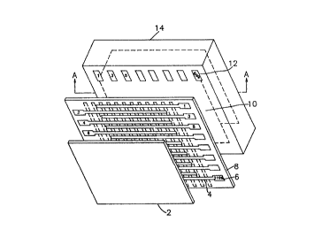
FIG. 1 is an exploded view of the structure of a
conventional electrophoretic display panel in which the
present invention is utilized.
FIG. 2 is a schematic sectional view of the grid,
cathode, and anode of the conventional panel shown in Fig. 1
taken along view lines A-A.
~ . .
W093/0~98 PCT/US91/05918
~115152 _4_
FIG. 3 is a schematic diagram of the X-Y
matrix control of the conventional electrophoretic
display panel.
FIG. 4 is a front view of a segmented anode
of an embodiment in accordance with the invention
showing a multiplicity of anode line segments.
FIG. 5 is an electrical circuit diagram of a
preferred switching circuitry for individually
controlling the anode line segments.
FIG. 6 is a timing diagram showing the line
erase mode for the display apparatus of the invention.
FIG. 7A and 7B are diagrammatic views of the
manner in which each anode line segment is aligned
with the cathode.
Best Mode for Carryinq Out the Invention
Referring to Fig. l, one type of
conventional electrophoretic display apparatus, in
which the present invention can be utilized, comprises
a glass plate 2, a plurality of cathode row conductors
4 having contact pads 6, a photoresist layer 8, a
plurality of grid column conductors lO having contact
pads 12 and another glass plate on which the anode 14
is formed. The exploded view of the display apparatus
in Fig. l is shown substantially out of scale for
purposes of illustrating the conventional grid,
cathode, and anode arrangement and explaining the
application of the invention. Fig. 2 shows a cross-
sectional view of this arrangement taken along view
lines A-A in Fig. l, and employs common reference
numerals for the common elements shown therein.
The glass plate 2 is coated with an
extremely thin layer of indium-tin-oxide (ITO), e.g.
approximately 300 angstroms in thickness, so that the
glass plate 2 remains transparent. The plurality of
W093/0~98 2 1 1 5 1 5 2 PCT/US9l/~9l8
row conductors 4 and associated contact pads 6, while
shown as residing on one side of the photoresist layer
8, are actually etched from the ITO layer coated on
the glass plate 2 through conventional photoetching or
engraving techniques. The row conductors 4 are
arranged as horizontal lines of the cathode for the
display, with each row having a given width and being
spaced by a given separation from adjacent rows. For
a display having a resolution of 200 lines per inch,
each cathode line may have a width of the order of 112
um and a separation of 15 um.
The photoresist layer 8 is formed over the
row conductors 4 while leaving the contact pads 6
exposed for forming electrical connections therewith.
The photoresist material may typically take the form
of phenolic resin impregnated with a photoactive
material. Thereafter, the photoresist layer 8 is
overcoated with a thin layer of chrome from which the
plurality of column conductors 10 and associated
contact pads are formed through conventional etching
techniques. The column conductors are arranged as
vertical lines for a grid of the electrophoretic
display. The column conductors are each formed with a
plurality of parallel tines which establish wells for
the electrophoretic particles and obtain the desired
color and contrast properties of the display.
Typically, each column conductor may have 4 tine
elements each of which has a width of 10-15 um and a
spacing therebetween of 20 um. Once the chrome layer
of column conductors with tines has been formed, the
base layer of photoresist 8 is removed in all areas
between the tines not having chrome thereon to form
wells 22 between the tines, as best shown in Fig. 2.
W093/0~98 PCT/US91/05918
2115152 -6-
In the conventional apparatus of Fig. l, a
unitary planar anode 14 may be formed by an ITO layer
on a glass plate. The anode wall is sealed to the
front glass plate 2 to form a fluid-tight enclosure 24
by which an electrophoretic dispersion of charged
electrophoretic particles in a suspension fluid is
contained. The grid and cathode lines are
insulatively separated by the photoresist layer 8 by a
spacing of the order of about 6 microns. The anode is
spaced from the cathode-grid wafer by a distance of
about 200 to 300 microns. These dimensions are
exemplary only and are given to indicate the relative
size and thinness of these structures. Each well 22
for retaining the particles is effectively formed near
the surface of each row conductor 4 intermediate each
tine of photoresist 20 underlying a conductor tine.
The display area is generally rectangular and may have
a total surface area equivalent to a standard 25 lines
of text characters or a full page size of 8.5 by ll
inches. For a more detailed description of this type
of electrophoretic display, reference is made to U.S.
Patent 4,742,345, which is incorporated herein. Other
types of electrophoretic display structures may of
course be used, for example, those having apertured
conductor lines for forming the particle wells, as
disclosed in U.S. Patent 4,655,897.
The conventional electrophoretic display
described herein is a triode device employing discrete
cathode, grid, and anode structures which enable
charged electrophoretic particles to migrate to and
from the wells formed between the cathode and grid
structures from and towards the anode structure. The
cathode and grid lines form an X-Y matrix which is
used to selectively impress a field on the particles
W093/0~98 2 1 1 ~ 1 ~ 2 PCT/US9l/0s9l8
--7--
in the desired pixel areas of the display. In order
to impress a field at a pixel of the X-Y matrix,
operating potentials are selectively applied at the
intersection point between the corresponding cathode
and grid lines, thereby impressing a field on the
particles retained in the well at that location.
If the cathode-grid structure is negatively
biased relative to the anode and the particles are
negatively charged, then application of operating
potentials to the X-Y intersection will cause
particles at that location to migrate to the anode,
thereby creating an image by the light color of the
particles at the anode against the dark color of the
suspension medium, or by the absence of particles at
the cathode. The particles may have a white or yellow
color, while the suspension medium may have a dark
grey color. While it is assumed herein that the
cathode lines are arranged in the horizontal direction
and the grid lines in the vertical direction, the
arrangement may of course be reversed. Those skilled
in the art will recognize that a display image may be
viewed at either the glass associated with the cathode
or that of the anode.
Referring to Fig. 3, a typical circuit
configuration is illustrated for applying operating
potentials to the X-Y matrix. The Y-drivers include
amplifier elements 72, 73 for applying voltages to the
Y-lines 70, 71 which are the grid lines in the above-
described display structure. The X-drivers include
amplifier elements 76, 77 for applying voltages to the
X-lines 74, 75 which are the cathode lines. The
driver amplifiers may be fabricated by conventional
integrated circuit techniques. Applying the proper
negative biasing potentials via the respective
15 2 -8- PCT/US91/05918
amplifiers while holding the anode at a more positive
"write" potential causes negatively charged particles
to migrate toward the anode. Conversely, applying a
more negative "erase" potential to the anode causes
the particles to migrate back toward the wells of the
cathode-grid structure.
A typical electrophoretic dispersion
consists of submicron particles of a suitable pigment
suspended in a fluid vehicle. The particles are
encapsulated by means of a charge control and wetting
agent which essentially coats the particles to enable
them to retain an electrical charge. The suspension
fluid wets the particles and allows them to be
suspended indefinitely in the vehicle. The vehicle
consists basically of a surfactant which contains no
water which would interfere with the electrical
operation of the panel. A typical electrophoretic
dispersion may include a yellow pigment such as AAOT
yellow, manufactured by Sun Chemical Company, for the
particles. A suitable vehicle employed with the
pigment is sold under the trademark CENTROLEX P, a
charge control and wetting agent which contains
lecithin. To this may be added tetrachloroethylene,
which is a vehicle solvent, plus a small amount of an
aromatic hydrocarbon as a wetting agent. A typical
particle composition contains 4% AAOT yellow, 0.16%
CENTROLEX P, 80.51% tetrachloroethylene, and 15.3% of
a hydrocarbon such as Aromatic 150 distributed by
Exxon Corporation. The yellow pigment particles
appear in high contrast to the dark grey color of the
dispersion to provide a very efficient display with
high visibility.
For an electrophoretic display having the
above-described dispersion, a voltage of about 1 to
W093/0~98 PCT/US91/05918
2115152
g
1.2 volts per micron of cathode-to-grid spacing is
required. Suitable displays have been operated in the
write mode by applying approximately +250 volts to the
anode, zero watts to the grid, and zero volts to the
cathode. In order to erase the display, the
potentials are reversed to make the cathode positive
with respect to the anode. A write or erase current
of about 85 microamperes can be used, thus consuming
very little power. Once an image is formed on the
cathode, it will remain there even after removal of
power. It is of course understood that other
dispersions having different pigments may be used,
such as a white pigment made of titanium oxide
distributed by Dupont Company under the trademark R-
101. A typical white pigment dispersion may consistof 10% R-101, 0.25% CENTROLEX P, 8% copper oleate of
4% concentration, and 81.75% tetrachloroethylene.
The present invention is particularly
directed to an improved anode structure for an
electrophoretic display which allows erasing of a
selected line without erasing the entire display,
thereby allowing a new frame having substantial
portions the same as the previous frame to be written
in less time. Referring to Fig. 4, an anode 14
comprises a multiplicity of individual anode conductor
segments 62 which are separated by a small spacing
from each other. In accordance with the preferred
embodiment of a display for primarily 24 lines of text
characters at a time, there are 24 conductor segments
62a through 62x in the form of elongated rectangular
strips in parallel and electrically insulated from
each other. The height of each conductor segment
corresponds to the height of a character line of the
display.
W093/0~98 PCT/US91/05918
2115152
As each anode segment is insulated from each
other, one or more anode segments can be switched to
an erase potential while the other anode segments are
maintained at the write or hold potential. The result
is that one or more character lines of the displayed
image can be erased while the other character lines
are not affected. Accordingly, only the erased line
or lines need to be rewritten to complete the next
frame of the display. After the line is erased, the
segment is returned to the hold potential and the
erased line is rewritten.
The selective switching of one or more anode
segments to the erase potential is accomplished by the
anode switching circuit depicted in Fig. 5. Three 8-
channel high voltage switch units 20, 22 and 24 are
connected in series to a data input DIN TOP by way of
an amplifier 32. Similarly, another three 8-channel
high voltage switch units 26, 28 and 30 are connected
in series to a data input DIN BOTTOM by way of an
amplifier 34.
In the preferred embodiment, each high-
voltage switch unit is an HV1616P chip made by
Supertex Inc. Each HV1616P chip has an 8-bit shift
register coupled to an input terminal DIN and output
terminal DOUT and an 8-bit latch in response to a
latch enable signal received on input terminal LE.
The input terminal DIN of the switch 20 is coupled to
the data input DIN TOP; the input terminal DIN of the
switch 22 is connected to the terminal DOUT of switch
20; and the input terminal DIN of the switch 24 is
connected to the terminal DOUT of switch 22.
The state of switch elements SW1 through SW8
of each of the high-voltage switch units 20, 22, and
24 is determined by the data input at DIN TOP. A
W093/0~98 2 1 1 5 1 ~ 2 PCT/US91/05918
--11--
train of 24 bits is shifted into the three 8-bit shift
registers, and the switch elements SWl through SW8 of
each unit is set by latching the input bits into their
respective latches. Depending on whether the
respective input bits are high or low, the
corresponding switch elements SW1-SW8 of the switch
units 20, 22, and 24 are independently opened or
closed. Similarly, the switch units 26, 28, and 30
are connected in series to the data input DIN BOTTOM
10 to latch the respective bits of the 24-bit input train
to their respective switch elements and independently
open or close the switch elements SW1-SW8 of each of
the three switch units.
Each switch element of the switch units 20,
15 22, and 24 couples a corresponding one of the anode
segments 62a through 62x to the +HV (write or hold)
voltage source by way of a 10-volt Zener diode 40 and
a corresponding 10 kilo-ohm resistor of the DIP banks
44, 46, and 48. Similarly, each switch element of the
20 switch units 26, 28, and 30 couples a corresponding
one of the anode segments 62a through 62x to the -HV
(erase) voltage source by way of a 10-volt Zener diode
42 and a corresponding 10 kilo-ohm resistor of the DIP
banks 50, 52, and 54. For normal writing and erasing
25 of the 24 character lines of the display, all anode
line segments 62a through 62x are connected to the +HV
and the -HV potentials, respectively. However, in the
selective line erasing mode, a selected anode segment
is connected to the -HV voltage source to be erased.
30 That is, in the case where all 24 lines have been
written and only one or more line(s) is (are) to be
erased to form a new frame, only the selected anode
segments are disconnected from the hold potential +HV
and connected to the erase potential -HV, while the
W093/0~98 PCT/US91/05918
211~1~2 -12-
others are maintained at the hold potential. Thus,
the DIN TOP signal must be the complement of the DIN
BOTTOM signal. To rewrite the selected lines, the
corresponding anode segments are then disconnected
from the -HV erase potential and reconnected to the
+HV hold potential.
The foregoing complementary signal control
of the respective rows of high-voltage switch units is
coordinated by a clocking signal sent from the CLK
input to the CLK terminals of the six switch units by
way of amplifier 36. The switch elements of all
switch units are all set simultaneously by a common
latch enable signal sent from the LE input to the LE
terminals of each of the switch units by way of
amplifier 38.
The waveforms in Fig. 6 show an example of
the selection of an individual line to be erased by
control signals supplied from the interface to the
panel switching circuitry. The signal LINEPTR points
to the line to be erased. In the example, the signal
LINEPTR indicates that the fourth character line is to
be erased. Note that only three pulses are necessary
since the signal is normally pointing to the first
- line. The LINEPTR signal is used to generate the
complementary 24-bit DIN TOP input signal with only
the bit in the fourth anode segment position low, and
- the DIN BOTTOM input signal with only the bit in the
fourth anode segment position high. The ERLINE signal
is then sent, the latch enable LE input signal is
generated, and line four is erased. The LINERDY
signal is sent when the line is ready to be rewritten.
In this example, it is assumed that each character
line is comprised of 26 scan lines. Thus, the data
bank for the display sends 78 RTS signals to the panel
W093/0~98 2 1 1 5 1 ~ 2 PCT/US91/05918
interface (each RTS signal is answered by a CTS
signal) to skip the first three character lines.
Following the 79th RTS signal and upon receipt of a
CTS signal, the data bank sends the desired line data
to the cathode and grid lines for rewriting the fourth
character line.
Use of the 24-segment anode of the invention
requires alignment of the cathode lines and the anode
segments each of which extend horizontally in parallel
with respective ones of the other. The assembly
procedure adopted involves laying the top of the first
anode segment directly in line with the top of the
first cathode line. As shown in Fig. 7A, most of the
cathode line 1 has transparent indium-tin-oxide (ITO)
on it, while both ends, i.e. the chip mounting end and
test comb area, are covered with chrome. Due to the
high reflectivity of the chrome surface, both ends of
the cathode line are visible, and adjustment of the
anode line 1 to its proper position over the cathode
line is facilitated. The anode segment is adjusted
until the chrome appears as a line continued over the
top of the anode segment, as shown in Fig. 7B. Slight
movement of the anode segment in the direction of the
arrows is used to obtain alignment. Although there is
some parallax due to a typical 14-mil spacin~ between
the cathode and anode, this causes an error of at most
only a few mils in practice. Significant twist error
is unlikely since the lines are typically 7 to 8
inches from end to end.
The above-described embodiments of the
invention are intended to be illustrative only, and
many other variations and modifications may be made
thereto in accordance with the principles of the
invention. All such embodiments and variations and
W093/0~98 PCT/US91/05918
2115152 -14-
modifications thereof are considered to be within the
scope of the invention, as defined in the following
claims.