Note : Les descriptions sont présentées dans la langue officielle dans laquelle elles ont été soumises.
-
2 ~ 2 7 9 1 ~
i
SPECIFICATION
Title of the ~vention
LAYERED STRUCI'URE COMPRISING lNSULATOR
S T~llN FILM AND OXlDE SUPERCONDUCTC)R THIN
F~LM
Background of the ~vention
Field of the invention
The present invention relates to a layered sll"clu-e COIllpl;5iUg an
insulator thin film and an oxide superconduc~or thin film, more
specifi~ ~lly, to a layered SllUClUIG COn~pliSil~g an insulator thin film and
an oxide superconductor thin film with a little interdiffusion at an
int~ e between those two thin filrns
Dcso.iyli~ll of related art
Oxide ;,~ e.~oluluctors which have been recently advanced in study
have higher critical temperablres t~an those of metallic ~ e-c~-n~ ct~rs
so that dley are more applicable ~or practical usage. For example,
Y Ba-Cu-O type oxide su~ .4on~ ctor has a critical ~ e-4lu-G higher
than 80 K and it is announced that Bi-Sr-Ca-~-O type oxide
~u~e~onductor and Tl-Ba-Ca-Cu-O type oxide superGon~ ct~r have
critical ~llly~:la~UI~,S higher ~an 100 K.
In order to apply the oxide superco~duc~ors to superconl1uctin~
devices, i~ is nkces~"r~ to make oxide supc~ d~etors in a form of
films. The term thin films means films, having a thirl~nçss of from 10-1
n~nrJme~rS to on the order of lû ,um, artificially depGsiled on substrates.
- 1 -
- ,: .. .
- . . . .
2~,27~
The oxide superconductvr thin films are usually deposited on single
crystal substrates, for examp]e a MgO substrate, a SrTiO3 substrate, a
YS~Z (yttrium stabilized zirconia) s.ll,s~.ale, etc., by various m~thod~ such
as a spuLIe- ing, an MBE (molecular beam epitaxy), a reactive
S co-evaporation, a CVD (chemical vapor deposition). The oxide
~u~)e~on~ tor thin filrns grow epitaxially on these substrate.
I~ is also necessary to deposit other thin films on the oxide
supelcon(l11ctQr thin films in order to manu~eLure some types of
~u~e~col~ cting devices. Forexample, a tuMel type Jose~h~ol- junction
10 CO~ S~S a layered structure of a ~Irst superconducting layer, an thin
insulator layer and a second sup~r~ondl1ctin~ layer stacked in the named
order. Therefore, if an oxide ~.lperc.)"dl1c1or is applied to the tulmel type
Josephson j11nction device, a first oxide su~)e~con-h~ctQr thin film, an
inSut~or ~in film and a second oxide su~G~o~ ctnr thin ~11m should be
1 5 stacked in the named order.
A su~)ercollducting field effect device, a candidate of realistic
three-t~rminol sù~elco~--lucting devices, has a supe,col-d11ctin~ channel
and a gate electrode forrned on d~e supelcol-d~Gtin~ channel throug}l a
gate jn~ul~tor layer. If a superconducting field effect device is
2 0 m~n~ t11red by using an oxide su~Jc;~o~ ucl( r, it is necess~ o stack an
oxide superconductor thin film, an insulator thin film and a normal
con~ ctor film in the named order.
In addition. in order to fabricate a s.~vGIconducting multi-layer
wiring structure by using an oxide su~rco1-Au-tor, oxide ~u~ con'h~ g
2 5 ~in films and insul~tor thin films should be alternately stacked.
A}l of above su~)e,~ollducting devices and elçmPnt~ require high
quality ~in ~lms. Namely, oxide supe,-,o~ uctor ~in films and o~er
2~ &
.
dlin fillllS preferably should have excellent prope~ties originated by their
high crystallinity. It is more preferable tha~ ~e thin films are fonned of
single crystals. If one of the ~in films is polycrystalline or amolphous,
the device or the element may have degraded characteristics or may not
5 even operate.
Additionally, in the above sul~ercond11cting devices and elenl~nt~,
;nl~.rhceS between the two difrelent thin films are also i,.ll)o,ia,ll. It iS
preferable that there is no inlerdirrusion through the interfaces, ille~c;fol~,
there should exist clear buundaly planes. In particular, if constituent
10 elern~ntc of the nonsuperconductor thin filrns diffuse into the oxide
superconductor thin films, superconducting properties of the oxide
.lpc.col~ductor thin films are fairly degraded, and vice versa.
In a prior art, all the thin films co~ of the layered structu~e
are deposited by using the same apparatus in order to prepare a layered
15 structure having clear interfaces. For example, in case of reactive
co~ pola~ion using ~Cnudsen cell (K cell) evaporation sources, an oxide
s~pelcol ~uctor thin film is deposiled on a ~ubs~ e at ~Irst, and then, the
other evaporation sources are used so as to deposit an insulator thin filrn
on the oxide supercond1~ctor thin film successively. A surface of t}le
20 oxide ~upel~;ollductor thin film, namely an interface l~tween the oxide
.lpe~ nctf~r thin film and the insulator thin film, is not exposed to ~e
air so as to be ~ en~d from cont~min~tion and degradation.
However, during the above process, the insulator thin film should
be deposited at a suitable substrate temperature for forming a highly
25 cryst~lli7.~d and, therefore, high quality insulator thin film. At this
rela~ively high substrate ~~ alure~ significant inle~i~rusion is caused
at the jn~rf~ce, main1y because of its long deposition time. By this, both
- 3 -
. ~ . , ~ .
:: : :: ':
; ~
!
the oxide superconductor thin film and the insulator thin film are
degraded so as to have poor qualities or properties.
I~ the insulator thin film is deposited at a lower substrate
l~ alulc: in order to avoid the iu~..li~îusion at the bolmdary plane, the
5 in~ tC!r thin film is less crystal]ine or may be formed of amorphous so
as to have ~legr~ d p~op~.lics.
Summ~ry of the Invention
Accordingly, it is an object of the present inYention to provide a
10 layered sll uelule comprising an insulator thin film and an oxide
su?eleo~-dllct~r thin film, which have overcome the above ~..P~ liolled
defects of the co~ intional ones.
The above and o~er objects of the present invention are achieved in
acco,-lance with the present invention by a layered structure formed on a
15 ~iubsllalt; co~ Jl;sillg an oxide superconductor thin film deposited on the
~b~ , a noble metal mono}ayer deposited on the oxide ~upercfu-.h~t~r
thin film and an insulator thin film deposited on the noble rnetal
monolayer.
The noble metal monolayer prevents illterdirrusion between the
2 0 oxide ~ ~o1u1~1ctor thin film and the insulator thin film. Therefore, ~e
layered structure in accor~ance with the present invention has a clear
boundary plane and no i~ rusion at the interface between the two
films.
According to the present invention, the noble metal monolayer must
2 5 be used. A crystalline noble metal layer ~thicker than monolayer~, even if
it is extremely thin, deposited on the oxide sul,tl~;onductor thin ~llm has
-j an periodic lattice structure of inherent lattice parameters which are
- 4 -
., _ , ,~ ~
~ 12 ~ 91 ~
~different from those of the oxide superconductor and those of the
insulator. Therefore, an insulator thin ~llm deposited on the thick noble
metal layer can not be epitaxially grown so as to be less crystalline so that
its properties are degraded.
On the o~er hand, the noble metal monolayer has le~s ability to
', affect a lattice structure of a thin film growing on it. Therefore, ar
in~ or thin film deposited on the noble metal monolayer can be g~own
up to m~int~in its inherent lattice parameters, so that a crystalline and
high quality insulator thin film can be obtained. For this pulpose, a noble
metal monolayer must be used in acco~a"ce with the present invention.
Preferably, the layered ~LIuC~ulc: further com~lsillg a buffer layer
~t~..ecll the substrate and the supercon~uctor thin film. The purpose of
this buf~er layer is to cc,lllycllsale lattice mi.cm~t-~.h between the ~.lb,~ r-and oxide superconductor and to prevent inte~lirrusion. For eY~mp1P' the
15~ buffer layer is formed of PrlBa2Cu307.y oxide. PrlBa2Cu307 y oxide has
a crystal ~lluelur~ similar to that of YIBa2Cu307." oxide ~ul Gl~co~lductor
so that the buffer layer of PrlBa2Cu307 y oxide can co~ )en~ate lattice
mi.~m~teh between the substrate and the YIBa2Cu3o7 ~ oxide
' ~u~e-collductor thin fflm. In addition, the buffer layer l.lltiY~
2 0 interdiffusion between them. Even if constituent elements of
PrlBa2Cu307 y oxide buffer layer diffuse into dle YlBa2Cu307 x oxide
s~,perco~duct( r thin film, IJIOpG.liCS of the oxide s-lpe.col-dl1ctor thin
film are not affected.
In a plefell~d embo~iment, the oxide thin film is formed of
25 high-TC (high critical temperature) oxide ~I~pe~.;ol~ductor~ particularly,
formed of a high-TC copper-oxide type compound oxide sulle-~;o.~ r,
for example, a Y-Ba-Cu-O compound oxide ~u~cl-,ullductQr material, a
, ~ , . . ~ . . . ..
3 ~L ~
Bi-Sr-Ca-Cu-O compound oxide superconductor material, and a
Tl-Ba-Ca-Cu-O compound oxide supelcol~ductor material. - ~ -
In addition, the substrate can be formed of an ;nc~ t;n~ substrate,
preferably an oxide single crystalline substr~te such as MgO, SrTiO3,
CdNd~104, etc. These substrate materials are very effective in forming ~ - -
or t'~~~Willg a crystalline film on them.
The above and other objects, features and advantages of dle present
invention will be apparent from the following descripti~n of pl~;re~ d
embo~liments of the invention with reference to the accolllpanying
1 0 dfhW~ ,S.
Brief Description of the Drawings
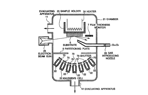
Figure 1 is a diagr~mm~ti~ sectional view of a film deposition
a~palatus which can be used for mAnl~facturing the layered ;.~l~clu~ in
1~ acco-dallce with ~e present invention; and
Figures 2A to 2E are diagr~mm~tic section~l views illustrating a
process for m~nllf~ctl~ring the layered structure in accordance with ~e
present invenltion~
20 Description of the Preferred embodiments
Referring to Figure I there is shown a dii~r~rnm~tir~ section~l view
of a film deposition apparatus which can be used for conducting the
process in acco~al~ce with the present invention.
This film deposition apparatus includes a vacuum ch~mber 21
25 provided with evnrl~tin~ appalaluses 11 and 12, seven K cells ~ having
~ontrollable shutters 70 provided a~ the bottom of the ~acuum c~ ber
21, and a sample holder 23 provided at ~e top of the vacuum cl~ ke~ 21
'7~r~ t ~)
I
~or holding a substrate 6 on which a film is to be deposited. Shutterg 70
and ~Illpe~ures of the K cells 22 are independently controlled so that ~e
- amount of molecular beam flux of each material and deposition rate of
co~ ound films,are independently controlled. The sample holder 23 is
5 ~ tPd to a heater 24 for heating the ~sL~ale and a thermocouple (not
shown). A film thickness monitor 7 is provided near the san ple holder
23. ln ;~ ion~ the vacuum Pl~n,~r 21 also has an electron beam gun 25
of ReflPetin~ High Energy Electron Diffraction (RHEEI~ e~u~ n~,nL
for observing roughness and crystallinity of a thin film even dunng the
10 deposition. Though not shown, a liquid nitrogen shroud for cooling outer
shells of the K cells 22.
Additionally, a gas introducing nozzle 26 is provided so as to
introduce an oxi~ n~ gas such as ~2. O3, NO2, N20, etc. to the vicinity
'of the subs~atP- 6 attached to the sample holder 23, so that the o~
15 gas can be supplied to forrn an oxygen-enriched atmosphere in the vicinity
of the substrate 6 in order to oxidize metal rnolec~ r beams supplied
~, - from the e~/al,olation sources in the course of the film ~ osili~,n.
' ' Fulllle.lllore, the film deposition apparatus additionally includes apartitioning plate 8 for dividing the vacuum clh~,~.ber 1 into a bottom
20 sub-çh~mhPr which consists of a lower por~ion of the Yacuum ch~mbçr
defined below ~e partit~ ng plate 8, which has the K cells 22 and the
main ev~ Atii~ appar~tus 12, and a top sub-~1 ,.ber which consists of an
upper portion of the vacuum c~ .e~ defined above lhe p~ ionil~g plate
8 and in which sample holder 3 is located. ~he partitioning plate 8
2 5 im~ s a round shape opening formed at a center thereof. The position
of the opening is determined to ensure ~at molecular beams emitted from
K cells toward the ~ul~sllal~ 6 are not obstructed by the par~itiot in~ plate
- 7 -
.. . .
' 21~79~
:: '
8. In addition, the size of ~e opening is determined ~o enab}e ~s~ d
oxygen leakage from the top sub-c~ her to the bottom sub-Gh~mb~r so
that a ~ICS;>l.lc difference can be created between these two sub-ch~ml~e~
Thelcrolt;, the partitioning plate 8 having the round shape opening acts as
5 a vacuum co~ el~U~e.
In addition, the evacnatin~ apparatus 11 is conn~cted to the top
sub-~h~-..her for evn~l~ating the top sub-chamber to an ultra-high vacuurn.
lhe auxiliary ev~~n~ting al,l,alalus 11 is co~ d of a cryopump. On
the other hand, the ev~cu~ting a ~ alus 12 iS conctit~t~d of a diffusion or
10 turbo pumps.
Referring ~o Figures 2A to 2E, a process for forming the layered
strueture in accorJ~ce with the present invention will be described.
As shown in Pigure 2A, an oxide buffeir layer 2 of prlBa2cu3o7-y
having a thickness of 30 nanometers was d~,posil~d on a SrTiO3 single
15 crystalline substrate 6 by reactive co-evaporation method. At ~irst,
SrTiO3 (100) substrate 6 was ~tta~hed to the sample holder 23, and metal
praseo~lyllliull., metal yttrium, metal barium~ copper, metal stlo-~liu.l.,
metal tit~illm and Au were put into tant~hl~ crucibles held within ~e
seven K cells 20 used as evaporation sources. Thereafter, inlets of ~e
20 rh~nber 1 were closed and evacuation process by the evacllating
appara~uses 11 and 12 began to reach an ultra-high vacuum which
obtained a p-~,s~-~ie lower than 1 x 10⁻¹~ Torr, which was required to
dle ba~,-ou.Jd pressure during the filrn deposition by the MBE process.
Succeerlin~ly, an oxidizing gas of ~2 including more than 70 volume
2 5 percent 03 was supplied from the gas introducing no~zle 26 so that the
oxi~ation gas partial pressure around the substrate 6 became 5 x 10⁻⁶
Torr.
- 8 -
.. .. .. . ~
2 1 h- S ~ 3
As ment~oned above, the vacuum eh~ er 1 was provided with the
vacuum ccn~ ct~nce ~the partitioning plate 8), a plessu~e dirrelellce of
about one digit or more was created between the bottom sub-ch~l,.k~ and
the top sub-chamber. Oxidation gas partial pressure of the bottom
S sub-rh~mher was maintained low enough to prevent the evaporation
sources from n~ i7~tion and to m~int~in the metal molecular beams from
each e~al~o~dLion source during the deposition. In ~(lition~ the oxidizing
gas injected from the gas introducing nozzle 6 was supplied onto a
sl,ccill,cn surface, the partial pressure of the oxidizing gas on the
10 deposition plane of the specimen was mqint~ined enough amount for the
oxide film formation~
Then, the substrate 6 was heated by the hea~er 4 to a ~rl~ of
650 ~C. The K cell 22 of metal praseodymium was heated to a
te~ crdlure of 920 ~C, the K cell 22 of metal barium was heated to a
;nl~el~lu~ of 620 ~C and the K cell 22 of metal copper was heated to a
~ clalul~; of 1000 ~C. The ~ al~ ,s of the K cells are (lete~ d
by the amount of metal molecular beam fluxes requested by the
a~ ...en~ of the MBE al~l>a,alus and oxide composition.
When molecular beams had reached to their stable operation, the
~0 shutters 70 were opened so as to start deposition of the Pr~Ba2Cu307.y
oxide thin film onto the substra~e 6. At the same time, surface
crystallinity of this deposited film surface was observed by the RHEED
device~
Then, all the shutters 70 of the K cells 22 were closed and dle K cell
2 5 ~ of metal yttnum was heated to a ~ t~itule of 1220 ~C~ At the same
dme, the substrate l~ Lule was raised to 700 ~C~ Other con~itinnQ
were kept ~e same~ When molecular beams had reached to their stable
g
. . . _ . .
'; ' ' ' ' - ', ,. ' ' .
'' . . ~ ..
2 ..L ~
v~-alion, a~ain, the shutters 70 of the K cells 22 of yttrium, barium and
copper were opened so as to start deposition of a YlBa2Cu307.;~ xcl)
oxide superconductor thin film 1 onto the PrlBa2Cu307.y oxide buffer
layer 2, as shown Figure 2B. At the same tirne, sl~rface cr~stallini~ of
5 this clepos;led film was obse. ved by the RHEED deviee.
PrlBa2Cu307 y oxide has a crystal structure similar to that of
YIBa2Cu307 x (0<x<1) oxide superconductor so that the oxide buffer
layer 2 of PrlBa2Cu307.y oxide moderates lattice mi~m~iite~r bei~,e,l ~e
SrTiO3 ~ub~llaL~ and d~e Y~Ba2Cu307.x oxide ~u~eJ-;onductor tbin film 1.
10 In addition, the buffer layer 2 prevents in~. liîrusion between them.
Even if co~..cl;l"e~-t element~ of Pr~Ba2Cu307 y oxide buffer layer 2 diffuse
into ~e YlBa2Cu307.,~ oxide s ipe..;o~ ctor thin film 1, p,u~c.lies of dle
oxide ~ el~io~ ot~irthinfilm 1 arenotaffecte~i-
When the YIBa2Cu307.,~ oxide superconduc~Qr thin film 1 was
15 grown up to have a thieltne~s of 10 nano,-.e~el~, all the shutters 70 of ~e
-K cells 22 were closed and the K cell 22 of Au was heated up to a
~e~ tul~; of 500 ~C. At the same time, the o~idizing gas was stopped
so that ~e chrimber 21 was evacuated to a pressure of 1 x 10⁻⁹ Torr.
After Au Inrol~c~ r beam had reached to its stable operation, the ~hutter
2 0 70 of the K cell 22 of Au was opened so as to s~art deposition of an Au
monolayer 3 onto the YIBa2Cu307 x oxide ~u~e.conducitor ~in film 1 at
dle suhs~tP le~llpe~a~ Of 700 ~C, as ~shown Figure 2C. l~e monolayer
3 can be formied of a noble metal which does not react with the oxide
?ll~elco~ etor, for example Au, Ag, Pt. If Pt is used as the noble mietal
2 5 monolayer 3, an electron beam gun is used as deposition source instead of
a K cell.
'i .
- 10-
.. .. . ~
. . .
2 :L 2 ~
.. . . ..
Thereafter, the shutter 70 of Au K cell 22 was closed and the K cell
22 of metal sLI~nliulll was heated to a temperature of 520 ~C and the K
cell 22 of metal ~ ni",n was heated to a lenl~cl~tu~e of I500 ~C. In
~d~liti~n, an nxi(1i7in~ gas of ~2 in~ ing more than 70 volume percent
5 03 was again supplied from the gas introducing nozzle 26 so dlat the
. .pl~ UlC; around the substrate 6 became 5 x 10⁻⁶ Torr. When rnOlpcul~
beams ~ad reached to their stable operation, the shutters 70 were opened
' so as to start deposition of the SrTiO3 insulator thin film 4 having a
~ ~hirlrn~ of 50 nanometers onto the Au monolayer 3, as shown in Figure
10 2D. ~e substrate t~ peldlulc was kept 500 ~C. The in~ tr, r laye~ can
be formed of SrTiO3, MgO or s~licon nitride.
~ situ observation with the RHEED device made it clear that the
SrTiO3 insulator thin film 4 was deposited sequel~ti~11y, which was
formed of a SfIiO3 single crystal, and had an uniform ~ ..ess
l 5 Then, all the shutters 70 were closed again and the K cell 22 of Au
was heated to a îe~ ature of 500 ~C. At the same time, the oxidi7.i
gas was stopped so that the ch~ 21 was evacuated to a ~s~u.e of
3 x 10⁻¹~ Torr. After Au molecular beam had reached to its stable
' operation, ~e shutter 70 of the K cell 22 of Au was opened so as to star~
2 0 ~ ~s;l;o~- of an Au layer S having a lI,irl ,If ~c of 200 r D ~OF~ ~ onto the
SrTiO3 in~ tor thin film 4 at a substrate 1e~ e~lu~e of 500 ~C, as
ishown in Figure 2E.
In situ obsc~v&tion with the RHEED d~vice made it clear ~at the
- 'Au thin film S was grown to satisfy a single crystalline con~ition
2 5 After the layered structures of the PrlBa2Cu30~ y oxide buffer layer
2, YIBa2Cu307 ,~ oxide SUyc.col ductor thin film 1, Au monolayer 3,
SrTiO3 dlin film 4 and Au layer 5 were obtained, crystal ~llu~;lul~,s iand
. . , . !,,
1 2~,i'~1 ) -
,
conditions of the interface were evaluated by SEM, LEED and XPS
without exposing the layered structure to the air. It became clear ~at the
YlBa2Cu307 ,~ oxide ~u~l-;onductor thin ~llm 1, the Sl~riO3 thin filrn 4
and Au layers 3 and 5 were formed of single crystals a~nd the h~te~rdc~s
5 ~I-.vel~ them were sharply formed with little i,~ dif~ ion~ Thel~role,
the layered structures had a small amount of intr~ce s~ates. By this, it
was favorable that a gate structure of a ~7u~l-,on~ ctin~ field effect device
was formed by the medlod in accordance with the present invention.
In ~e above process, if the seven K cells can not be set in one
10 chamber, it is possible to use an apparatus co~ isillg equal to or more
than two c~mbers and in situ sample transfer device conl~ectin~ the
chambers.
In addition, the layered structure according to the present invention
can be applied to a structure having a thin film of an arbitrary material
15 deposited on a ~in film of an oxide ~upe.cundoctor.
Fu~ e~ ore~ the oxide ~ ereo~lductor thin film can be formed of
a high-TC (high critical temperature) oxide sul)efcol~ductor m~tr~ri~
particularly a high-TC copper-oxide type con~l~Gul~d oxide ~u~)e'~ionrll~ctor
material, for example a Ln-Ba-Cu-O (Ln means a l~nth~noide) c~ d
2 0 oxide supelconductor material, a Bi-Sr-Ca-Cu-O compound oxide
superconductor material, and a Tl-Ba-Ca-Cu-O compound oxide
supercoll~nl~tor material odler than YlBa2Cu3~:)7.,~ oxide ~ulJe~on(luc~or
material.
The thin film deposited on $he oxide superconductor ~ lm can
2 ~ be formed of an arbitrary material .lirrere~lt from the oxide
~.lpe.co~dllctQr, for example, an in~ or such as SrTiO3, MgO, silicon
!
, - 12-
~,
.,.. , .; ; , .~ , .. . . .. .
, ~ 1 . . .
. , i: . ~ .
2 ~ J ,~
ni~ride, a semiconductor, an oxide supe~conductor, an oxide such as
; PrlBa2Cu307 y etc.
llle su~ can be fonned of for example, an in.~ tor ~ te
such as a MgO (100) substrate, a SrTiO3 (100) substrate, a CdNdAl04
5 (001) !7~ Sl~t~: or others.
The invention has thus been shown and described with ~cr~ cc to
~e specific embo~1iment.c. However, it should be noted that the present
:invention is in no way limited tO the details of the illustrated structures
but COII~/G~l~ and modi~lcations may be made within ~e scope of ~e
10 appended claims.
: ..
,~ .
- 13-