Note : Les descriptions sont présentées dans la langue officielle dans laquelle elles ont été soumises.
2128839
-- 1 --
OP~ICA~ MODULATQR8 A~ MO~CT.T~ICAL~Y 1~. 1 ~vNAT~D ORTICA~
ISOI~5~0Rg
T~h~ic~l Field
This invention relates generally to ~ method and
apparatus for use in high-speed optical fiber data
transmission systems. More particularly, the present
invention relates to a configuration of modulators for
providing a timed sequence of optical gates that allow
data pulse transmission in a forward direction and
attenuate all signals travelling in the reverse direction.
The device can therefore function as an optical isolator,
and i9 suitable for monolithic integra~ion with other
semiconductor components in an optical data transmission
system.
sach~ul~d o~ th~ Invention
When several optical components are connected in
tandem, an optical isolator is usually required to
suppress instability of the optical source. Such
instability may be caused by light reflected back into the
optical source by a neighboring component, or by light
originating ~rom a different source that impinges on the
optical sourc~e.
Prior art optical isolators typically rely on the
non-reciprocal nature of magnetic media to achieve
isolation. These current devices rely on a polarization
rotation or non-reciprocal beam deflection, and with ti~e
invar.iant syi~ems this non recipxocal behavior is required
,~ by defi.nition. Other approaches, such as using a linear
polari~er in conjunctlon with polarization components that
-~unction a~ ~uarter-wave plates, re~uire that the
reElection being isolated against is a non-polarization-
changing reflectiorl. Therefore, if the reflected signal
is in an arbitrary polarization,state, the reciprocal
,
2~2~;39
,
.; - 2 -
isolation means discussed above are inadequate. Further,
interfering light from a different source may have an
., .
arbitrary polarization state. Thus, any time-invariant
reciprocal means cannot in general provide isolation.
It is known that directly modulated semiconductor
laser sources suffer from frequency chirp problems due to
the inherent fluctuations of the complex index of
refraction that are used to induce the modulation.
Semiconductor electroabsorption modulators using bulk or
quantum well structures have been developed to mitigate
such frequency chirp problems, and monolithically
integrated devices comprising electroabsorption modulators
and distributed feedback lasers (DFB lasers) or
distributed Bragg re~lector lasers (DBR lasers) have been
. 15 demonstrated. See, Eor example, Y. Noda et al., "High-
Speed Electroabsorption Modulator with Strip-Loaded
'; GaInAsP Planar Waveguide", IEEE J. Liqhtwave Tech., Vol.
LT-4, pages 1445-53 (1986), and M. Suzuki et a]..,
"Monolithic Integration of InGaAs/InP Distributed Feedback
Laser and Electroabsorption Modulator by Vapor Phase
Epitaxy", IEEE J. Liqhtwave Tech., Vol. LT-5, pages 1~79-
85 (1987). For very high bit rate systems of 10 Gigabits
i per second or higher, however, even the small amount o~
~rec~ency chlrp exhibited by a monolithically integrated
laser and electroabsorption modulator clevice can degrade
system per~ormance. A significant component of the chirp
in such a device can result from undesirable re~lectlon~
from the modulator output facet. In addition, reflec~ions
Erom adjoining components may cause system clegradation
when an external modulator is used to encocle the
unmodulated output o:E a laser source Eor high-speed, long
~; clistance optical Eiber ~ata transmisqion.
Although the monoli.thic inte~ration of optical
devices on the same semiconductor substrate has many
advantages including reduced connection losses, increased
..
~;'
:'
" 2~288~9
-- 3
reliabili~y, lower cost and lower power consumption, due
to the reciprocal properties of semiconductor materials
and the requirements for isolation outlined above, it has
not previously been possible to effectively integrate
optical isolators and light sources. Consec~ently, both
reflections Erom adjoining components and light
; originating Erom other sources may degrade the overal].
performance of the light source.
~ummary of th~ v~ io~
It is an object of the present invention to provide a
method and apparatus resulting in an optical isolator that
is suitable for use with semiconductor light sources. The
optical isolator can be monoli.thically integrated with an
optical source resulting in a device having reduced
frequency chirp characteristics, suitable for high-speed
optical fiber data transmission.
It is a further object of the present invention to
protect against light interference ~rom other sources and
from any reflections of the transmitted signal.
One embodiment of the invention comprises at least
two modulators arranged sequentially in a line through
which signals from a signal source propagate. The
moclulators are arranged to have a spatial separation
chosen to realize a sequence of timed "open gates" that
are qynchronous with the traveling wave of a return-to-
zero (RZ) bitstream of data from the source. The term
: ~open gate" is defined as the ~unction o~ a moclulator
whereb~ it is in a transmissive state, and the term
"closed gate" is i.ts attenuating state. In particular,
each modulator in the sec~ence is driven to have a periodidentlcal to that o~ the RZ pulse stream, and the phase of
tho drive to each modulator is chosen so that a modulator
oEfers an open gate delayed in time from the preceding
modulator's open gate by the propagation delay between the
:
. .
CA 02128839 1998-0~-26
modulators. The timing of the open gates coincides with the
bit period of the emitted RZ pulse stream, such that data is
transmitted without attenuation in the forward direction.
Further, the timing of open gates is such that a signal
traveling in the reverse direction will encounter at least
one modulator that is in its off state, presenting a closed
gate. The degree of attenuation of such a signal depends
upon the extinction ratio of the modulator. Therefore,
isolation is provided from any signal traveling in the
reverse direction, including reflections and signals from
other sources in the system. The device is suitable for use
as an optical isolator for a semiconductor light source, and
further may be monolithically integrated with the light
source.
Another embodiment according to the present invention
comprises a sequentially arranged modulator and a passive
waveguide for connection to a signal source. The passive
waveguide provides a propagation delay for any signal
reflected by the end facet of the waveguide, such that the
modulator attenuates the reflected signal before it impinges
on the source. This configuration substantially reduces
frequency chirp for an optical transmission system, and can
be monolithically integrated with a light source. Although
this embodiment provides isolation only from the end facet
reflections, in some circumstances this is the most
troublesome signal to isolate against. Thus, this
configuration may be the simplest, smallest, and most cost
effective isolator embodiment.
In accordance with one aspect of the present invention
there is provided a monolithically integrated signal source
and isolator apparatus for providing a stable, low frequency
chirp source device for high-speed fiber-optic data
transmission, comprising: a laser light source utilized as
the signal source; a first modulator driven to be
synchronous with a transmitted data stream from the signal
source; a second modulator driven to be synchronous with the
transmitted data stream, wherein the second modulator is
CA 02128839 1998-0~-26
- 4a -
sequentially arranged and spaced a distance apart from the
first modulator to provide a phase delay between them, and
wherein the modulators generate a timed sequence of open
gates which permit transmission of a data signal in a
forward direction and attenuate a reverse direction signal;
and a semiconductor substrate, with the laser light source
and the first and second modulators monolithically
integrated on the semiconductor substrate.
In accordance with another aspect of the present
invention there is provided a method for providing isolation
for a stable, low frequency chirp signal source for high-
speed fiber-optic data transmission, comprising: connecting
a first and a second modulator to said signal source while
monolithically integrating the first and second modulators
and said signal source on a semiconductor substrate;
sequentially spacing the second modulator at a distance from
the first modulator to provide a predetermined time delay;
driving the first modulator to be synchronous with a
transmitted data signal from the signal source to produce a
first sequence of open gates; driving the second modulator
to be synchronous with the transmitted data signal to
produce a second sequence of open gates, wherein the second
sequence of open gates is delayed in time from the first
sequence of open gates; transmitting data signals in a
forward direction through the open gates of the first and
second modulators; and attenuating a reverse direction
signal.
Brief Description of the Drawinqs
Fig. 1 is a simplified block diagram of two modulators
positioned to operate as an isolator according to the
present invention;
Figs. 2 and 3 are timing diagrams illustrating the
operation of the apparatus of Fig. 1;
--' 2128~39
- 5 -
Fig. 4 is a simplified block diagram illustrating a
cross-sectional view of an integrated source and isolator
device according to the present invention;
Fig. 5 is a timing diagram for an embodiment
utillzing a plurality of modulators to form an isolator
according to the present invention;
Fig. 6 is a simplified block diagram illustrating a
cross-sectional view of an integrated source and isolator
device according to another embodiment of the present
inventioni
Fig. 7 graphically illustrates the transmissivity of
the modulator of Fig. 6 and the re~lected light intensity
as a function of time; and
Fig. 8 gxaphically il~ustrates the effective
reflectivity of the end facet of the device of Fig. 6 as a
function of passive waveguide length for different
extinction ratios.
Detalled Descri~ion
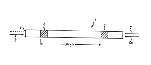
Fig. 1 is a simplified block diagram of an isolator 1
according to one embodiment of the invention. Although
the present invention is described herein in the context
of optical data trainsmission systems, it should be
understood that the apparatus and technique can be applied
to other transmission systems.
Referring to Fig. 1, a first modulator 2 is
sequentially arranged with a second modulator 3 so as to
be separated by a d.istance L. For the purposes of this
application, a modulator is defined as any device capable
; o~ altering the intensity or amplitude oE a signal. One
end 4 of the isolator 1 can be attached to a signal source
~not shown), such as an optlcal source. Isolator 1
permits a transmitted signal S to propagate through the
- modulators 2, 3 without being attenuated, as shown by
arrow 5a. A reverse direction signal 7 is attenuated by
. .
,j,
~.
,,., ~128g3~
-- 6
the isolator 1 before it can impinge on the source, thus
preventing transmission system degradation due to
inter~erence from other sources and from signal
reflections.
Figs. 2 and 3 are timing diagrams which respectively
illustrate forward direction transmission of a data signal
21 through the isolator 1 of Fig. 1, and attenuation of a
reverse direction signal 26. It should be understood that
Figs. 2 and 3 are not drawn to scale, and are presented in
this manner to facilitate understanding of the invention.
It should ~urther be understood that the transmission and
attenuation operations shown separately in Figs. 2 and 3
can occur simultaneously.
In the discussion of Figs. 2 and 3, it i5 assumed
that the isolator 1 of Fig. 1 is connected to an optical
source (not shown) which transmi~s a Return-to-Zero (RZ)
modulated data bit stream having a period T with a data
bit rate of B=1/T. Referring to Fig. 2, a data pulse 21
is shown travelling with a group velocity vq in a forward
direction 20 through "open gates" 22, 23 generated by each
of the two modulators 2, 3. llhe term ~open gate" is used
here to refer to the function of a modulator whereby it is
in an open, transmissive state, and the term ~clcsed gate~
is its attenuating or blocking state.
Referring to Figs. 1 and 2, the first modulator 2 is
driven to provide a Eirst series of open gates 22 of
duration T~, and the second modulator 3 is driven to
provide a second series of open gates 23 o~ duration T~J.
The open yates 22, 23 are synchronous with the RZ
modulated data bit stream generated by the source. The RZ
data stream pulses are o~ duration Tp, which is less than
one-halE oE the period oE the data bit stream,
Tp c T/2. Each oE the open gates 22, 23 has a duration T~
that is longer than the duration Tp of a data stream pulse
~288~
-- 7
21, and does not exceed one-half of the bit period. Thus,
Tr~ S Tg S T/2.
In addition, the modulators are arranged to have a
spatial separation of L = vgTd, as shown in Fig. 1, so
that a time delay of Td exists between them with respect
to the arrival time of a pulse at each modulator.
Fig. 3 depicts the same set of generated gates shown
in Fig. 2, however, a signal 26 travelling in a reverse
direction 25 is shown being attenuated by the isolator 1
10 of Fig. 1. The signal 26 is shown propagating Ereely
through the middle of the open gate 23 of the second
modulator 3. As the signal 26 continues in the direction
25, it encounters the closed gate 24 of the first
modulator and is attenuated. This attenuated pulse is
depicted as dotted line 26a. The degree of attenuation oE
a reverse direction signal is a function of the extinction
ratio of the modulators. Thus, the degree of isolation
provided by an isolator according to the present invention
depends upon the type of modulators utili~ed.
Referring to Fig. 3, in order to assure that all
reverse direction signals are attenuated, the timing of
the open gates 22, 23 must be such that the first
modulator's open gate 22 must close before any reverse
direction signal making its way through the beginning of
the second modulator's open gate 23 reaches the first
modulator. Thus, it is required that 2Td 2 T~. This
; condition guarantees that such a signal will be attenuated
by a closed gate of the ~irst modulator. In addition, the
Eirst modulator cannot have its next open gate 22' ~or the
next cycle until after any reverse direction signal 26
passing through the tail end o~ the second modulator's
open gate 23 is attenuated. This requires that twice the
clelay Td plus the duration of an open gate T~ be equal to
,i or less than the period of the data signal, or 2Td + T
T. Thus, i~ the delay T~ between open gates 22, 23
,'' :
'
2~28839
- 8 -
satisfies the expressions Td ~ Tg/2 and Td < (T~Tg) /2, then
data pulses 21 will be transmitted without attenuation in
the ~orward direction 20, while all reverse direction
signals 26 will be attenuated.
The two conditions Td 2 T~/2 and Td S (T-Ty)/2 arise
from the requirernent that no signal can ~et through in the
reverse direction. If both conditions are not met, then
part or all of a reverse direction signal could make its
way through the modulators and impinge upon the source.
10 In high speed flber optic data transmission systems, such
interference is undesirable. For example, lt could ca~se
frequency chirp problems which can degrade system
performance.
Flg. 4 is a simpliEied block diagram illustrating a
15 cross-sectional view of an integrated source and isolator
device 40 according to the present invention. A dotted
line 46 represents a semiconductor substrate and other
layers utilized to Eabricate such a device. A detailed
illustration of the various semi.conductor layers is beyond
20 the scope of the present application, and one of skill in
the art knows that such a monolithically integrated device
would comprise a number of layers requ.iring many
r fabrication steps.
Re~erring to Fig. 4, a DFB laser 41 and two
25 modulator~ 42, 44 are monolithically integrated on a
semiconductor substrate 46. In this embodiment, a light
signal from a continuously operating, unmodulated DFB
laser 41 is encoded with an RZ pulse pattern by modulator
4~ as it travels in the direction oE data transmlssion
inclica~ed by arrow 48. The two modulators 42, 44 are
driven by drivers 43, 45 to Eunction in the manner
described above, and both can be driven by the data signal
i provided the timing sequence satisfies the expressions Td
> Tg/2 and Td S (T Tg) /2. The device 40 has immunity to
external signals traveling ln the reverse direction back
,~ .
!~.
.,
~ 12,~39
towards the laser source 41, and also immunity to
reflections from the end facet 47 of the device. Thus,
the embodiment of Fig. 4 provides a stable, low fre~uency
chirp RZ source device suitable for high-speed fiber-optic
data transmission. For the purposes of this application,
high-speed data transmission is defined as being a gigabit
per second and higher.
The particular embodiment shown in Fig. 4 preferably
employs electroabsorption modulators 42, 44 as the optical
isolator and a DFB laser as the light source 41. The
electroabsorption modulators provide low-loss transmission
in a lower voltage "on" state, but provide high absorption
and thus attenuation in a higher voltage l~off" state. It
should be understood that other modulators, such as
directional coupler modulators, Mach-Zehnder modulators,
waveguide cut-off modulators, or other interferometric
modulators may also suitably be employecl. In addition, a
single driver may be used for both modulators as long as a
phase delay is introduced to provide properly timed open
and closed gates as explained above. Further, other laser
sources such as DBR semiconductor lasers may suitably be
used.
While Fig~. 1 to 4 illustrate a two modulator
isolator device, more sophisticated modulator sequences
using more than two modulators can readily be constructed.
Fig. 5 is a timing diagram 50 illustrating how the
present techn~que can be generalized so that many
modulators with a spatial separation of v~Tcl between each
modulator can be utilized. Fig. 5 illustrates the
sequence oE open gates for five modulators having a
duration T~ and period T. The period oE the RZ pulse 52
ls ec~ual to the period T oE the modulator gates, and the
duratiorl of a pulse in the data stream T~ is less than the
duration Tg of an open gate. The phase of the drive to
each modulator is such that the modulator has an open gate
r
~2~
- 10 -
of duration Tg delayed in time from another modula~or~s
open gate. This delay is the propagation delay Td between
the modulators, and Td is a function of the spatial
separation of the modulators from one another. Thus, the
modulators are arranged sequentially in a line so that the
timing of their open gates are synchronous with an RZ
modulated data pulse stream to allow propagation through
the modulators in the forward direction, indicated by
arrow 53. Conversely, a signal travelling in the reverse
, 10 direction 54 will encounter at least one modulator in the
seguence which is in the lloffll state or presenting a
closed gate. It should be ~Inderstood that, in practice,
modulators have some spatial extent, which can add some
propagation delay to the data signal as it passes through
a modulator. Thus, when the modulators are sequentially
arranged, thls propagation delay must be included in the
calculation of the net propagation delay between each
modulator.
When a plurality of modulators form an isolator, it
is not essential that all of the modulators satisfy the
criterion Td 2 T~/2 and Td < (T-T~)/2, as long as at least
i, two of the modulators comply. However, if each of the
', modulators in the sequence does satisfy the expressions Td
~ 2 Tg/2 and T~ ~ (T-T~)/2, wherein T~ represents the delay
,, 25 from the preceding modulator, then a signal traveling in
the reverse direction will be made to experience more ~han
one clo.sed gate, or modulator in its off state.
~ ReEerring to Fig. 5, a signal 55 traveling in the
reverse direction 54 will be attenuated when all or part
oE ~he signal encounters a closed gate. Thus, reverse
direction si~nal 55 is attenuated by closed gate 56
g~ne~ated by th~ fourth modulator, and is further
attenuated by closed gate 58 generated by the third
modulator. This phenomenon is illustrated by dotted lines
, 35 57, 57~, 57'~ and 57''~ which become lighter to represent
.; . .
i~.
.
!'.,
2~2~83~
- 11
diminishment of the reverse direction signal. Thus, when
q more than one closed gate is encountered higher isolation
is achieved, resulting in improved performance.
The above timing diagram examples illustrate
5 isolation of an RZ data bit stream that is already
encoded. However, the first modulator in the sequence can
provi.de the means for encoding the light source signal
with an RZ signal. Since the modulator must be in the
"on" state for transmission of the data pulses, if there
10 is no pulse to be transmitted during a particular bit
period T (i.e., a "zero" in a string of "ones" and
"zeros"), then the modulator will be off for a full cycle,
and khus still provide isolation during the re~uired part
of the timing cycle. Thus, it is possible for a modulator
15 to encode the data signal on an unmodulated light beam if
the modulator is driven with the RZ data signal. In fact,
each modulator in the isolator sequence can be driven with
the RZ data signal as long as the appropriate time delays
are maintained between the modulator drive signals.
In some high-speed fiber optic data transmission
devices, the end facet of the device produces reflections
which cause frequency chirp problems. Several attempts to
overcome the frequency chirp problem have failed because
available facet
anti-reflection coatings are inade~uate. The embodiment
of Fig. 6, discussed below, specifically addresses this
problem.
Fig. 6 is a simplified schematic diagram illustrating
, ~ a cross-sectional view o~ a monolithically integrated
isolator 60 ~or reducing the frequency chirp problem
caused by reflections Erom th~ end Eacet 52. A dotted
line 61 represe~ts a semiconductor substrate and other
layers utili~ed to Eabricate such a device. A detailed
illustration of the various semiconductor layers is beyond
the scope of the invention, and ,one of skill in the art
,,.
~12~&39
,
; - 12 -
knows ~hat such a monolithically integrated device
comprises a number of layers requiring many fabrication
steps.
Referring to Fig. 6, a passive waveguide 6~ has a
length L and is integrated with an electroabsorption
modulator 66 and a DFB laser 68. The modulator 66 is
connected to a driver 65, and is driven to be synchronous
with an RZ modulated data stream. The passive waveguide
64 functions as an optical delay line for light reflected
~rom the end facet 62. In particular, the length I, of the
passive waveguide 64 provides a round-trip propagation
delay time for the reflected light that is one-half a
modulation bit period, or an odd-number multiple thereof.
The length o~ passive waveguide 64 thus should be L=
Nv~/~4B), where N is an odd integer, vg is the group
velocity o~ an RZ signal in the passive waveguide and s is
the bit rate. For a monolithically integrated device, a
short delay line having N=1 is desirable. Fig. 7
depicts the transmissivity 70 of the modulator 66 of Fig.
6, and the reflected light intensity represented as dotted
line 72, as a ~unction of time. If the length o~ the
passive waveguide 64 is correctly chosen, then the
modulator is in the "o~~" state when the reElected light
72 ~rom the end facet 62 impinges on the modulator 66.
Consequently, the reflected light signal 72 is attenuated
and is not coupled into the DFB laser 68.
It is important to recognize that the ~requency chirp
induced by reElections from the end facet 62 is
proportional to the re~lectivity Ro of the end facet.
Thu~, the modulator 66 is used to eE~ectively reduce the
reflectivity o~ the end facet 62, as explalned below.
The transmissivity of an el.ectroabsorption modulator
a~ a ~unction o~ applied voltage V(t) can be characterized
, by the exponential function T(V(t)) = exp{-0.23xn
V(t)/Vp~}, where Vpp is the peak to peak applied voltage
,, .
.
.,
~ r:. -
~ .
- 212~ 9
. . .
- 13 -
; and n is the extinction ratio in decibels. The extinction
ratio is defined as the on/off intensity ratio of the
transmitted ligh~ pulses, and a large extinction ratio is
desirable because if the signal has such a characteristic
' 5 it is then easier to accurately decode the transmitted
' data. An extinction ratio of more than 30 dB has been
experimentally obtained for electroabsorption modulators.
For example, for an RZ data stream the effective
~' reflectivity Reff can be defined as the amount of reflected
light coupled into the source laser, which is averaged
over one modulation period. Thus, the reduction ratio is
R~ff/Ro = ¦ T(V(t))xT(V(t-td))dt, where Ro is the power
reflectivity of the end facet, and td is the propagation
; delay time provided by the passive waveguide, which is: td
= 2L/Vg~
Assuming that the applied voltage is described by the
simple sinusoidal function V(t) = Vpp {l~cos(2~Bt)}/2,
then, from the above equations, the relationship between
the effective reflectivity and the length of the passive
waveguide can be obtained.
Fig. 8 graphically illustrates the effective
~ reflectivity of the end facet 62 as a function of passive
; waveguide length for different extinction ratios. As
shown, when the passive waveguide 64 provides a delay time
of one half a modulation bit period (or an odd-number
~' multiple thereof), the effective reflectLivity is
j;' dramatlcally reduced. For example, the effectivq
~ reflectlvity is reduced by a factor o~ more than 150 when
;,~ the extinction ratio is 30 dB. The length of the delay
line is dependent on the bit rate. For example, for a 10
Gigabit per seconcl RZ modulated signal, the lencJ~h L of
th~ pa~ivo waveguide should be approximately 2mm. In
addition, i~ a low-loss semiconductor passive wavecJuide is
used, then insertion losses should be negligible.
I
:~,
t
~!
,
2 1 2~39
- 14 -
Use of a passive waveguide in the manner described
above may also be helpful for ~educing the reflection-
induced frequency chirp problem when other types of
modulators and laser sources, such as Mach-Zehnder
modulators and DBR lasers, are utilized.
The apparatus and methods disclosed herein provide
for isolation oE a source against signals travel:Lng in the
reverse direction that may impair its performance. By
monolithically integrating two or more modulators with a
light source, a device can be realized which isolates
against light signals from externai sources, as well as
from reflections. By inteyrating a single modulator and a
passive waveguide, a device can be realized that isolates
against reflections of the light source from a known
point, such as the end facet. Calculations show that the
e~fective re~lectivity in this case can be reduced by a
factor of more than 150 when the extinction ratio is 30 dB
Eor a transmission system using an RZ modulation signal.
Thus, the present invention dramatically relaxes the
requirements on anti-reflection coatings at an end facet,
and further enables a booster semiconductor amplifier to
be integrated into a laser source and modulator device
without significant increase in the frequency chirp.
Further, the proposed concept could be extended to reduce
optical feedback due to reflections in large scale
photonic integrated circuits.
It should be understood that the above described
arrangem~nts are only examples of embodiments of the
invention. It w.ill be apparent to those of skill in the
art that various changes may be made without departin~
~rom the spirit and scope o~ the invention.