Note : Les descriptions sont présentées dans la langue officielle dans laquelle elles ont été soumises.
2142~gO
309-924150-NA
DUAL MODE TRANSMISSION SYSTEM WITH
SWITCHED LINEAR AMPLIFIER
BACKGROUND OF THE Ihv~NllON
Field of the Invention
The present invention relates to dual mode radio frequency
transmitters, and more particularly to a dual mode
transmitter having a to-and-from transmission path
including a switched linear amplifier responsive to a mode-
of-operation control signal.
Description of the Background Art
U. S. Patent 5,121,081 issued January 9, 1992 to Hori
entitled "OUTPUT WAVEFORM CONTROL CIRCUIT" discloses an
output waveform control circuit for a time division
multiple access system, including a second driving circuit
which sends a control signal to the power amplifier in
accordance with a signal outputted by the comparator
circuit. Thus, by controlling the operating voltage of the
power amplifier simultaneously with the control of the
level input signal from the input level control circuit,
the output characteristic of the power amplifier, including
a class C or the like amplifier having a non-linear
input/output characteristic, is prevented from varying
abruptly, and the output waveform of the power amplifier is
so controlled as to have gently sloped leading and trailing
edges.
U. S. Patent 5,060,294 issued October 22, 1991 to Schwent
et al. entitled "DUAL MODE POWER AMPLIFIER FOR
RADIOTELEPHONE" discloses a dual mode power amplifier
operable in either the linear mode or the saturation mode.
The power amplifier, when comprising a portion of a radio
transmitter, permits efficient amplification of either a
2142540
-
frequency modulated or a composite modulated signal by
operation of the amplifier in the saturation mode or the
linear mode, respectively. A processor determines the
modulation-type of the signal and generates a signal to
cause operation of the amplifier in either the saturation
mode or the linear mode.
U. S. Patent 4,955,083 issued September 4, 1990 to Phillips
et al. entitled "DUAL MODE RADIO TRANSCEIVER FOR AN SSB
COMMUNICATION SYSTEM" discloses a radio transceiver for use
in an SSB communication system having FM data capability.
The dual-mode radio transceiver of the present invention
incudes a receiver capable of demodulating and deriving AFC
from either the voice channel having voice messages
transmitted via single sideband amplitude modulation with
a pilot carrier, or the data channel having high speed data
messages transmitted via narrowband frequency modulation in
the same channel bandwidth. Furthermore, the dual-mode
radio transceiver includes a transmitter capable of
transmitting one of either of the above types of modulation
on the appropriate channel, as determined by information
received from the high speed data messages transmitted on
the control channel.
U. S. Patent 4,924,191 issued May 8, 1990 to Erb et al.
entitled "AMPLIFIER HAVING DIGITAL BIAS CONTROL APPARATUS"
discloses an amplifier equipped with a digital bias control
apparatus to provide precise, dynamic control over the
operating point of a plurality of amplifying elements in
the amplifier. A processor optimizes the operating point
of each individual amplifying element as a function of the
amplifying element characteristics, the operating
environment and the applied input signal. The use of a
processor also enables the user to remotely program the
operating point of each individual amplifying element in
the amplifier. The processor further enables dynamic
changes in the operating characteristics of the amplifier
as the operating environment of these amplifying elements
~142540
-
changes. The processor also generates an alarm signal if
any particular amplifying element is operating out of its
nominal specifications. This digital bias control
apparatus can function in class A, AB, B or C type of
amplifiers whether they are tuned or untuned and whether
the amplifier operates in a pulsed or continuous mode.
U. S. Patent 4,446,440 issued May 1, 1984 to Bell entitled
"DUAL MODE AMPLIFIER" discloses an apparatus that amplifies
the signal in a linear mode when the voltage of the signal
is much less than the voltage of the power source, and in
a switching mode when the signal is at other voltages.
U. S. Patent 4,257,009 issued March 17, 1981 to Yorkanis
entitled "INHIBIT CIRCUIT FOR DIFFERENTIAL AMPLIFIER"
discloses a system wherein the outputs of a pair of non-
additive combiners are coupled to respective inputs of a
differential amplifier and an a.c. signal to be amplified
is applied to a selected input of one of the combiners. A
control circuit operates in a first mode to apply control
voltages to the combiner inputs for causing the one
combiner to block the a.c. signal and also causing both
combiners to apply a common mode input voltage of a first
value to the amplifier inputs. In a second mode, the
control circuit changes the values of the control voltages
in a sense to cause the one combiner to pass the a.c.
signal and to also cause both combiners to apply a common
mode input voltage of a second value to the amplifier
inputs whereby, in either mode, the amplifier produces a
constant quiescent d.c. output voltage.
U. s. Patent 4,03~,308 issued July 5, 1977 to Wermuth et
al. entitled "AMPLIFIER WITH CONTROLLABLE TRANSMISSION
FACTOR AND SWITCH~RT~ CONTROL CHARACTERISTIC" discloses an
amplifier circuit whose gain bears a desired relation to a
control voltage, including a differential amplifier, a
plurality of impedances interconnected between the
amplifier terminals and switches interconnected with the
~142S40
impedances and switchable between two states which create
two impedance configurations that give the circuit mutually
complementary gain vs. control voltage control
characteristics.
Japanese Patent 54-104760 issued August 17, 1979 to Hikari
Honda entitled "AMPLIFIER OF LOW POWER CONSUMPTION"
discloses a system a bias control signal circuit for an
amplifier to provide lower power consumption. The output
power is detected and a bias control signal is produced
that changes the operation point of the amplifier depending
on the transmission signal level.
European Patent Application number 90302627.6 filed March
13, 1990 by Vaisanen and published October 3, 1990,
entitled "A METHOD FOR CHANGING THE OPERATING CLASS OF A
TRANS~ K" discloses a method for changing the operating
class of a radio telephone transmitter used especially in
a gsm radio telephone system. When the transmitter
comprises one or several power stages of class A, B, AB or
C, it is possible according to the invention to change the
operating point of one or several power stage transistors
by means of a controlled semiconductor switch whereby the
class of the power stage amplifier changes to that desired.
SUMMARY OF THE INVENTION
It is difficult to provide a radio frequency transmitter
for use in mobile phone systems for broadcasting both equal
and non-equal amplitude high-frequency signals by means of
the same device (e.g. the DAMPS and CDMA transmission
systems to be referred to here as dual mode mobile phone
systems) which will achieve highest possible efficiency in
both operational modes. This is an especially serious
problem in the case of hand-held phones, which require a
high-efficiency transmitter in all modes of operation in
order to provide a long operating time and to minimize
warming caused by waste heat.
~ 21g2~40
-
The conventional solution of employing a linear transmitter
in which the same transmitter is used to amplify both equal
and non-equal amplitude signals, results in poor
efficiency, particularly in the case of transmissions which
use equal amplitude signals.
One solution previously used in the art for dual mode
transmission to improve efficiency is to provide a circuit
in which the operating point of the transmitter (and
thereby its efficiency) is adjusted in accordance with the
signal to be transmitted. In the case of the amplification
of an equal amplitude signal, the operational category is
adjusted to class C, for example, which provides a high
efficiency.
An object of the present invention is to provide a dual
mode transmitter for use in mobile phone systems which
produces a high efficiency in the case of both equal and
non-equal amplitude transmissions.
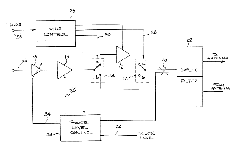
BRIEF DESCRIPTION OF THE DRAWING
The drawing illustrates a schematic block diagram of an
embodiment of a dual mode transmitter according to the
principles of the present invention.
DESCRIPTION OF A PREFERRED EMBODIMENT
Referring to the drawing, a dual mode transmitter circuit
is illustrated including a high-power amplifier means 10
having an amplification that can be adjusted and a linear
high-power amplifier 12. A first switch 14 and a second
switch 16 are connected to the input and output of
amplifier 12. An amplification-adjustable, high-frequency
transmitter control amplifier 18 is connected to the input
of amplifier 10. Means 20 for measuring transmission power
such as a directional coupler is connected to switch 16,
and a duplex filter 22 is connected to means 20.
~1~25~0
-
A power level control means 24 is responsive to the
measured transmission power from means 20 and to a power
level signal on lead 26. Power level signal on lead 26 is
representative of the desired output power of the
transmitter. The power level control means 24 compares the
measured power level from means 20 with the desired power
level on lead 26 and produces a difference signal on its
ou~L leads 34 and 35 and provides the difference signal
on leads 34 and 35 to both the high-power amplifier 10 and
to the high-frequency transmitter control amplifier 18.
The output of high power amplifier 10 can be controlled via
the power amplification operating point, the operating
voltage or the input operating power.
A mode selection signal, for designating either an analog
or digital type transmission mode is applied to terminal
28. A mode control means 25 is responsive to the mode
selection signal on terminal 28 and provides switching
signals to switches 14 and 16 and a control signal to
linear amplifier 12. Thus, the mode selection signal
applied to terminal 28 sets the transmitter to function in
either the non-linear transmission (analog) mode or the
linear transmission (digital) mode.
The modulated signal to be transmitted is applied to the
input terminal 36 of control amplifier 18, and passed
through high-power amplifier 10. If switches 14 and 16 are
set in the "a" position, which is the position for the
digital transmission mode, the modulated signal from
amplifier 10 is connected to and passes through linear
high-power amplifier 12, through power measurement means
(differential coupler) 20 and through duplex filter 22
where it is connected to an antenna (not shown) for
transmission.
For the non-linear, or analog mode of transmission, an
analog mode designating control signal is applied to
2142540
terminal 28. In response, mode control means 25 provides
signals on leads 30 and 32 which set switches 14 and 16 to
the "b" position, thereby disconnecting and removing
linear, high-power amplifier 12 from the transmission path
between amplifier 10 and duplex filter 22. The output of
amplifier lO is connected through coupler 20 to filter 22.
Amplifier 12 is in a non-active state. Amplifier 10 is
operated near or at it's saturation non-linear region to
achieve high enough output power and high efficiency.
The output power of the transmitter is controlled by
adjusting either the amplifier lO input power or the
operating voltage of an output transistor contained in
amplifier lO.
For the linear, or digital mode of transmission, the mode
control signal at terminal 28 designates a digital
transmission mode and causes mode control means 25 to
provide signals on leads 30 and 32 to place switches 14 and
16 in the "a" position wherein the output of amplifier 10
is connected to the input of linear amplifier 12. The
overall output power from amplifier 18 and amplifier 10 has
been set so low, that amplifiers 18 and 10 effectively
operate in a linear manner, for example with a-6dB back-
off, meaning that the input power of an amplifier isadjusted such that the output power is some 6dB below the
ldB compression point and thus the amplifier is operates in
a linear mode. Amplifier 12 receives such a low power RF
level input signal that it operates in a linear mode, that
is, in class A.
Thus, in the transmission system of the present invention
transmission power is adjusted in both the analog and
digital modes by measuring the output transmission signal
power with the directional coupler 20 and comparing it with
the desired output transmission power on lead 26 at the
power level control means 24. A differential signal is
used as a correction signal and is fed back to amplifiers
21~2~40
_
18 and 10.
A significant feature of the present invention is that the
same structures can be used in both the analog and digital
modes and that the output power in the analog mode can be
adjusted by regulating the gain of gain controllable
amplifier 18, or the amplifier 10 bias point or adjusting
the amplifier 10 operating point, or in some
implementations, the supply voltage. In the digital mode
the output power can be adjusted only be regulating the
gain of the gain controllable amplifier 18.
What has been described is a dual mode transmitter
structure that operates in an analog or a digital mode
depending on the state of a mode control signal. A linear
amplifier is connected in series into the transmission
signal path in the digital mode. It should be understood
that the switches are logical functions and need not be
implemented by physical switches. The switches 14 and/or
16 may be replaced in other implementations, for example by
power divider(s).
While the invention has been described in connection with
a preferred embodiment, it is not intended to limit the
scope of the invention to the particular form set forth,
but, on the contrary, it is intended to cover such
alternatives, modifications and equivalence as may be
included within the spirit and scope of the invention as
defined in the appended claims.