Note : Les descriptions sont présentées dans la langue officielle dans laquelle elles ont été soumises.
C A 2 1 4 3 64 1
Method of producing small components
The invention relates to a method of producing small components, in
particular pressure or similar sensors, which consist of at least two
individual units superimposed in layers.
Figures 1 a to 1c show a commonly known method of manufacturing such
small components 1. In a first method step (Fig. 1a), a silicon wafer 2 is
produced which includes a plurality of individual semiconductor units 5 or
wafer subunits 6. Fig. 1a shows a plan view and a perspective view of
such an individual semiconductor unit, all individual semiconductor units 5
produced on the silicon wafer 2 being similarly structured and regularly
arranged. An electrical circuit arrangement with connecting or terminal
spots 14 is arranged on the surface of an individual semiconductor unit 5.
Further, a shaped carrier part is produced which includes a plurality of
carrier subunits 7. The silicon wafer 2 and the shaped carrier part together
form a built-up wafer, the wafer subunits 6 and the carrier subunits 7 of
glass together forming the individual semiconductor units 5.
In a further method step (Fig. 1b), a plurality of individual connecting units
8 are produced. These individual connecting units 8 have, for example, a
projection 8-1 and a bore or recess 8-2 as shown in Fig. 1b. Following
manufacture of a plurality of such individual connecting units 8, the silicon
wafer 2 and the shaped carrier part are cut, for example,
C~2 1 43G~ l
with a diamond saw in order to produce a plurality of individual
semiconductor units 5 (Fig. 1 a) .
In two further method steps (Fig. 1c), all of the individual units 6, 7 and 8
are joined in order to produce the small components 5.
Thus, in such a method of producing components, as many individual
joining operations are necessary as there are individual semiconductor units
produced from the silicon wafer 2. In view of the fact that, for example,
200, 400 or 600 individual semiconductor units can be produced on one
wafer, this results in the corresponding number of individual joining
operations, which is very time-consuming, uneconomical and costly.
Additionally, the individual semiconductor units have extremely small
dimensions, for example 2, 3 or 4 mm edge lengths. Consequently, for
the joining operations indicated in Fig. 1c, an alignment of the water
subunit 6, the carrier subunit 7 and the individual connecting units 8 must
be carried out, but the gripping, aligning and joining of such small
dimensions is extremely difficult and time-consuming.
It is therefore the object of the present invention
to provide a method by means of which a plurality of small
components consisting of at least two individual units superimposed
in layers can be produced in a short time with little input of effort
and at low cost.
This object is solved in accordance with the invention by a method of
producing small components which is characterized by the following steps:
CA 2 1 4 3 6 4 1
a) producing a wafer with a plurality of individual semiconductor units;
b) producing a shaped connecting part with a plurality of individual
connecting units;
c) aligning the wafer and the shaped connecting part in such a manner
that an individual semiconductor unit respectively opposes an
individual connecting unit;
d) simultaneously joining each individual semiconductor unit with its
respective individual connecting unit, the wafer and the shaped
connecting part being maintained;
e) producing the small components by simultaneously separating the
wafer and the shaped connecting part along separating lines
between the individually joined individual semiconductor units and
individual connecting units.
In accordance with the invention, it is suggested to produce a shaped
connecting piece which has a plurality of individual connecting units.
Instead of the joining of individual semiconductor units with individual
connecting units individually, only one alignment of the wafer and the
shaped connecting part is necessary in accordance with the inventive
method. This provides the considerable advantage that only a single
operation step is necessary for connecting all individual semiconductor
units and individual connecting units. Consequently, it is no longer
necessary to individually align an individual semiconductor unit and an
individual connecting unit. So long as it is ensured that the individual
connecting units of the shaped connecting parts are arranged regularly in
the same manner as the individual semiconductor units on the waver, only
one alignment of the wafer and the shaped connecting part is
CA2 1 436d 1
necessary, which considerably reduces the production time (approximately
1/300). Thus, the work input is reduced, the production time is
considerably shortened and a considerably cheaper production of such
small components is thus possible.
An advantageous embodiment of the method according to the invention
can also be used in the production of small components which consist of
more than two individual units superimposed in layers in such a manner
that
- a wafer with a plurality of wafer subunits is produced,
- a shaped carrier part with a plurality of carrier subunits is produced,
- the wafer and the shaped carrier part with wafer subunits and
carrier subunits aligned with respect to each other are joined with a
plurality of individual semiconductor units consisting of wafer
subunits and carrier subunits to form a built-up wafer, and that the
steps d) and e) are carried out with the built-up wafer.
Thus, even when the small components are to be made up of several
individual units superimposed in layers, the manufacture by means of one
shaped carrier part makes it possible that only one alignment of the shaped
connecting part, the shaped carrier part and the wafer is necessary. Thus,
the manufacturing time and the manufacturing costs for the production of
small components which consist of more than two individual units
superimposed in layers is also reduced.
In the last-mentioned method of producing small components which
consist of more than two individual units, the shaped carrier part can be
joined with the wafer and the shaped connecting part simultaneously in
one step by means of their
CA21 43641
respective individual units. In this case, an alignment of the individual
units takes place first.
However, it is also possible to align respectively the wafer and a shaped
carrier part with respect to each other and to initially join these, after
which a further alignment of this stacked structure with the shaped
connecting part is carried out before joining these. As only one alignment
of a wafer, the shaped carrier part and the shaped connecting part is
necessary, the manufacturing time is substantially reduced also for the
production of small components consisting of more than two individual
units.
For the joining step to join the individual units of the wafer and the shaped
connecting part, or the shaped carrier part, a eutectic or anodic bonding
process or another suitable process can be used. This is particularly
advantageous because, in this method, it is not necessary to individually
gain access to individual semiconductor units Iying in a central portion of
the wafer. The wafer and the shaped connecting part must therefore
simply be aligned with respect to each other and moved towards one
another for the eutectic or anodic bonding.
In order to prevent stresses in the small components, it is advantageous if
the wafer, the shaped connecting part and possibly the shaped carrier part
are produced from materials which have the same or a similar coefficient
of thermal expansion. For example, the wafer is produced from silicon and
the shaped connecting part from glass, vacon or kovar, while the shaped
carrier part is made from glass or pyrex.
CA2 1 436~ ~
Following production of the small components, further joining steps can be
carried out in order to connect the small components with additional
holding elements. These further joining steps can include glass soldering,
adhesion, electron-beam welding for laser welding processes.
Advantageously, these additional holding elements also have similar
coefficients of thermal expansion as those of the produced small
components.
Advantageously, the small components are pressure sensors, the individual
semiconductor units being produced as elements exposed to pressure and
the individual connecting units being produced as connecting or terminal
elements.
In order to connect the small components with analysing electronics, it is
advantageous that in a further method step a connecting foil is applied
onto the individual semiconductor units of the small components in such a
manner with strip conductors along webs which lead to individual
terminals that these individual terminals come to lie in a contacting manner
on connecting or terminal spots of the individual semiconductor units.
In order to prevent stresses in the connection, the connecting foil consists
of a flexible material such as polyimide.
It is advantageous that the connecting foil is joined by means of adhesion,
soldering or tape-bonding to the individual semiconductor units or
contacted by means of other suitable connecting processes.
CA21 43~41
The connecting foil is formed with individual terminals, such as stamped
out terminals, in such a manner that it is ensured that there is the smallest
possible introduction of force onto the individual semiconductor units.
In the following, the invention is described in more detail with reference to
the drawings.
In the drawings there is shown in:
igs. 1 a to 1 c a commonly known production method for small
components which are made, for example, of three
individual units superimposed in layers;
igs. 2a to 2f a production method for small components according to
the invention;
igs. 3a to 3c an embodiment of an individual connecting unit which is
provided in the shaped connecting part shown in Fig. 2b;
igs. 4a and 4b a small component produced by means of the production
method according to the invention which is connected
with an additional holding element;
Fig. 5 an embodiment of the production method
according to the invention for producing small
components which are made up of more than
two individual units superimposed in.layers; and
CA2 1 43641
Fig. 6 an embodiment of the production method
according to the invention in which a connecting
foil, with conductor strips for the connection of
the individual semiconductor units by means of,
for example, four terminal points to analysing
electronics, is mounted onto the individual
semiconductor units.
In the following description of advantageous embodiments of the
invention, the reference signs denote the same or corresponding parts as in
Figs. 1 a to 1 c.
Fig. 2 shows a production method according to the invention (denoted full-
wafer production method in the following) for small components which are
made up of at least two individual units superimposed in layers. For
example, these small components are pressure sensors. Firstly, as in the
commonly known method (Fig. 1 a), a silicon wafer 2 is produced with a
plurality of individual semiconductor units 5 which are arranged in a regular
manner on the wafer 2 (Fig. 2a). Additionally, a shaped connecting part 4
is produced which includes a plurality of individual connecting units or
connecting or terminal elements 8 joined to each other. Fig. 2b shows a
top plan view and a perspective view of the terminal elements 8 arranged
in a regular manner adjacent each other in the shaped connecting part 4.
The number and size of the terminal elements 8 corresponds to the number
and size of the individual semiconductor units 5.
In a next method step (Fig. 2c), the wafer processed in this manner with
any desirable outer dimensions (typically 4") and the shaped connecting
part are aligned with respect to each
C A 2 1 43 6 4 1
other in such a manner that each individual semiconductor unit 5 opposes
a corresponding individual connecting unit 8. As the individual connecting
units and the individual semiconductor units 5 have the same size, only
two individual semiconductor units 5 and two individual connecting units 8
must be aligned with respect to each other. The number of individual
semiconductor units 5 produced on the wafer are therefore opposed by
exactly the same number of individual connecting units 8, with the same
dimensions as the Si-wafer, of the shaped connecting part, the respective
individual semiconductor units and individual connecting units being placed
in exact superposition with respect to each other.
As shown in Fig. 2, the silicon wafer and the shaped connecting part are
then joined to each other by means of a eutectic joining process or another
suitable joining technique, all opposing individual units being
simultaneously joined to each other. Thus, all individual semiconductor
units are joined with their respective individual connecting units in a single
operation step. The structure produced in this manner is shown in Fig. 2d,
Fig. 2e showing a side view of this layered structure.
In order to produce the individual small components (Fig. 2f), the layered
structure shown in Fig. 2d is cut along the separating lines 9, for example
with a diamond saw. In this case, the shaped connecting part 4 and the
wafer 2 as well as a shaped carrier part 3 are simultaneously separated.
The shaped connecting part 4 and the shaped carrier part 3 to be joined to
the silicon wafer consists, for example, of a material which has a similar
expansion coefficient to that of the silicon material (for example glass,
pyrex, vacon,
CA2 14364 1
kovar etc.). Thus, in joining the shaped connecting part, the shaped carrier
part and the silicon wafer, no unfavourable stress conditions are produced.
Fig. 3 shows an exemplary embodiment of an individual connecting unit 8which is particularly used for the production of pressure sensors. Fig. 3a
shows a perspective view, Fig. 3b a side view and Fig. 3c a top plan view.
The individual connecting unit 8 consists of a projecting part 8-1 and a
part with a bore 8-2. The part with the bore is provided for connection
with the individual semiconductor units 5 (see Fig. 2a).
As fig. 4 shows, the shape of the individual connecting units or terminal
elements 8 is appropriately selected for a further connecting process. This
connecting process for a larger holder can, for example, ensue by means of
glass soldering, adhesion in the case of terminal elements 8 consisting of
glass, or by means of electron-beam or laser welding (in the case of
terminal elements 8 of vacon or kovar) or by means of another similar
process. Figs. 4a and 4b show how the small components 1, consisting of
the individual semiconductor unit 5, which itself consists of a wafer
subunit 6 and a carrier subunit 7, and the individual connecting unit 8 can
be connected with such further holding elements 10 of a different material.
In this case, it is of advantage when the individual semiconductor unit 5,
the terminal element 8 and the further holding element 10 have similar
expansion coefficients in order to prevent stresses in the individual joints.
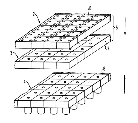
Fig. 5 shows an embodiment of the production method for small
components according to the invention. This embodiment is
Cll2 I 436~ 1
especially provided for small components which are made up of more than
two individual units superimposed in layers. In this method, in addition to
the production of the silicon wafer 2 and the shaped connecting part 4, an
additional shaped carrier part 3 is produced. This shaped carrier part 3
carries a plurality of carrier subunits 7 which correspond in terms of size to
the wafer subunits 6 of the individual semiconductor units 5 and to the
individual connecting units 8. The additional carrier subunits 7 of the
shaped carrier part 3 can be carrier parts, spacer parts, other electrical
circuits etc. In the method shown in Fig. 5, the wafer 2, the shaped
carrier part 3 and the shaped connecting part 4 are aligned with respect to
each other so that all respective individual units oppose one another.
In a further step, the wafer 2 is first joined with the shaped carrier part 3.
Following this, there is then the further joining to the shaped connecting
part 4. This can again take place by means of eutectic or anodic bonding.
Following this, the wafer 2, the shaped carrier part 3 and the shaped
connecting part 4 are simultaneously cut so that a plurality of small
components are produced which consist of more than two individual units.
Although an alignment of the wafer 2, the shaped carrier part 3 and theshaped connecting part 4 is carried out simultaneously in Fig. 5, it is also
possible to initially align the wafer 2 and the shaped carrier part 3 with
respect to each other, to join these together and then to align the
composite layers 2, 3 with the shaped connecting part 4 and thus join
these .
CA21 43641
12
A further advantageous embodiment of the method according to the
invention includes the application, for example by means of bonding or
another suitable contacting process, of a connecting foil 11 onto the
individual semiconductor unit 5 of the small components 1, as illustrated in
Fig. 6. The connecting foil 11 is shaped in such a manner, for example by
stamping out, that it has individual terminals 13 which correspond to and
lie opposite respective terminal spots 14 (see also Fig. 2a) on the individual
semiconductor units 5. The connecting foil 11 has strip conductors 12
along webs 15 which are connected with these individual terminals 13.
The strip conductors are, for example, connected with analysing
electronics for the small components 1. The connecting foil 11 is provided
separately for each small component 1 and has a circular shape with cut-
outs .
The connecting foil 11 is joined in such a manner that only the individual
terminals 13 come to lie on the respective terminal spots 14 of the
individual semiconductor unit 5. On account of the application of such a
connecting foil, a particularly stress-free joint between the individual
semiconductor units and the analysing electronics is produced. In this
case, it is advantageous when the connecting foil 11 consists of flexible
plastic such as polyimide. The shape of a connecting foil 11 with such
individual terminals 13 guarantees the smallest possible exertion of force
onto the small component 1.
The full-wafer production method according to the invention was described
above in connection with the production of pressure sensors consisting of
silicon wafers, but it is also suitable for the production of any kind of small
components.
~A21 43641
The full-wafer production method according to the invention is particularly
suitable for the manufacture of small components that have extremely
small dimensions, for example 2, 3 or 4 mm edge lengths, since the
individual alignment of individual semiconductor units and individual
connecting units is difficult for such small components. In an
advantageous manner, the invention avoids this problem by producing a
wafer and a shaped connecting part, the wafer and the shaped connecting
part simply having to be aligned with respect to each other and joined.
Thus, the method is cheap and makes the production of 200, 400 or 600
similar small components possible in the shortest time.