Note : Les descriptions sont présentées dans la langue officielle dans laquelle elles ont été soumises.
21481~9
WHEEL BALANCER DIGITAL OUTPUT FORCE TRANSDUCER
This invention relates to an apparatus for balancing rotary bodies,
5 such as the wheels of a motor vehicle, which is commonly referred to as a
wheel balancer. More particularly, the invention relates to a force
transducer assembly for use in such an apparatus which converts the
analog signal generated by the force transducer into a digital signal within a
shielded environment which is relatively impervious to electrical
1 0 interference.
Wheel balancers of both the motorized and hand-spun types are well
known in the automotive service equipment art. For example, U.S. Patent
No. 4,046,017, which issued to Hill and is owned by the assignee hereof,
15 discloses a motorized wheel balancer comprising a rotatable shaft upon
which the wheel to be balanced is mounted and a pair of force transducers
positioned adjacent the shaft for providing signals representative of the
imbalance forces on both the inner and outer rims of the wheel. The force
transducers employed in prior art wheel balancers are typically analog
20 devices, such as piezoelectric crystal load cells, which generate analog
signals which must then be transmitted to a central processor remote from
the transducers.
One problem with typical prior art analog force transducers is that
they are high impedance devices which output a low level analog signal that
25 is then transmitted to a converting and digitizing circuit connected to the
central processor. The converting and diyili~ g circuit presents a high
impedance load, and when the converting and digitizing circuit is located
remote from the transducers, the transducer signal becomes highly
susceptible to the electrical interference or noise commonly experienced in
30 the wheel balancer environment. This noise is usually eliminated using
either analog or digital filtering techniques. Also, if the high impedance load
results from the use of large values of resistance, DC drift due to
temperature and humidity become a problem.
These and other problems are overcome by providing a force
35 transducer assembly comprising a piezoelectric crystal transducer and a
21~81S9
transducer circuit board located within an electrically shielded housing. The
transducer circuit board comprises a operational-amplifier ("op-amp") circuit
and an analog-to-digital ('WD") converter. Thus, the force transducer
assembly is capable of generating a digital signal which is relatively
impervious to electrical interference, thereby eliminating the need for any
further filtering at the central processor. Preferably, the A/D converter is a
high resolution sigma/delta-type converter with a built-in low-pass filter
which guarantees 16 bits of monotonic data and effectively reduces the
transducer bandwidth to just above the expected shaft frequency to further
reduce system noise and allow the digital signal to more accurately
represent the actual analog force being measured. In addition, the op-amp
circuit preferably has a high input impedance. The use of the high
resolution A/D converter with the high input impedance op-amp requires
only one stage of analog amplification and no need for analog gain
adjustments. This greatly reduces errors due to DC drift with temperature
and humidity.
These and other objects and advantages of the present invention will
be made apparent from the following detailed description, with reference to
the accompanying drawings.
Figure 1 is a perspective view, partially broken away, of a wheel
balancer incorporating the transducer assemblies of the present invention;
Figure 2 is an exploded perspective view of the transducer assembly
of the present invention;
Figure 3 is a diagrammatic view of the transducer circuit of the
present invention; and
Figure 4 is a diagrammatic view of a second embodiment of a portion
of the circuit depicted in Figure 3.
While the force transducer assembly of the present invention may be
adapted for use in a variety of applications, it is particularly suitable for use
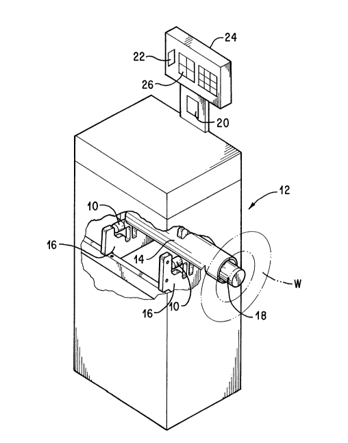
in vehicle wheel balancers. Referring to Figure 1, two force transducer
assemblies 10 according to the present invention are shown incorporated in
a representative vehicle wheel balancer 12. The particular wheel balancer
depicted in Figure 1 comprises a bearing tube 14 which is supported on two
2148i59
suspension brackets 16. In a manner known to those skilled in the art,
bearing tube 14 is adapted to receive a rotatable mounting shaft 18 to
which a wheel W is mounted for correction of unbalance. Suspension
brackets 16 are designed to yield in a direction transverse to the axis of
5 bearing tube 14, and force transducer assemblies 10 are mounted at
appropriate locations on suspension brackets 14 such that the forces
generated by the unbalance in wheel W as wheel W rotates are transmitted
through bearing tube 14 to force transducer assemblies 10. A more
complete description of the structure in which force transducer assemblies
t 0 10 are mounted is not critical to an understanding of the invention.
The digital signals generated by force transducer assemblies 10,
which will be described more fully hereafter, are transmitted to a central
processing circuit 20, which comprises a suitable microprocessor for
processing the digital signals and generating data indicative of the
15 magnitudes and locations of the wei~l ,ts required to be applied to wheel W
to correct the imbalance in wheel W. This data is transmitted to a suitable
display circuit 22 located in a console 24. Display circuit 22 controls the
presentation of the data on a visual display 26. Force transducer
assemblies 10, central processing circuit 20, display circuit 22 and a motor
20 control circuit (not shown) are preferably located remote from each other on
individual circuit boards to prevent any electrical interference generated by
each circuit board from affecting the other boards or force transducer
assemblies 10.
Referring to Figure 2, each force transducer assembly 10 comprises
25 a piezoelectric transducer element 28. In a preferred embodiment of the
invention, transducer element 28 is manufactured from a piezoceramic
material such as lead zirconate titanate equivalent to Channelite 5500 or
Navy Type ll (mil standard .1376 (ship)), which is silvered on both sides,
poled for compression loading parallel to its axis and has a diameter of .630
30 inch and a width of .042 inch to produce an output of 400 coulombs per
Newton of force with a capacitance of 2900 picofarads. Such a transducer
element can be obtained from a number of manufacturers of piezoelectric
devices, one of which is Piezo Kinetics Incorporated of Bellefonte,
Pennsylvania. Transducer element 28 is sandwiched between two contact
35 plates 30, each of which comprises a contact 32 which is soldered to an
-- 21~815~
appropriate junction on a transducer circuit board 34, which will be
described more fully hereafter.
Force transducer assembly 10 further comprises two insulator disks
36, which are manufactured from the same piezoceramic material as
5 transducer element 28, but not silvered or poled. Insulator discs 36 insulate
contact plates 30 from electrical contact with the respective raised bosses
38 of a top thrust plate 40 and a bottom thrust plate 42, both of which thrust
plates are manufactured of a metallic material such as steel. Transducer
element 28, contact plates 30 and insulator discs 36 are held together
10 between bosses 38 by a sleeve 44 manufactured from an appropriate
insulating material. Sleeve 44 comprises two slots 46 which are adapted to
receive contacts 32 to thereby allow sleeve 44 to be positioned around
contact plates 30. Transducer circuit board 34 is fastened to bottom thrust
plate 42 by screws 48. The appropriate spacing between transducer circuit
15 board 34 and bottom thrust plate 42 is maintained by standoffs 50. Screws
48 and standoffs 50 also serve to ground transducer circuit board 34 to
bottom thrust plate 42. A cable 52 comprising a number of wires 54
soldered to appropriate junctions on transducer circuit board 34 and having
a connector 56 attached to the distal ends of wires 54 provides for electrical
20 communication between transducer circuit board 34 and the central
processing circuit board 20. Cable 52 extends through an aperture 58 on
top thrust plate 40 and is secured to transducer circuit board 34 with a tie
wrap 60
Force transducer assembly 10 also comprises a cylindrical housing
25 62 into which top thrust plate 40 and bottom thrust plate 42 are slideably
received to thereby form a complete enclosure for the other components of
transducer assembly 10 described above. Housing 62 is preferably made
of the same metallic material as top and bottom thrust plates 40 and 42 to
provide an electrical shield for transducer circuit board 34. In addition, a
30 conductive silver epoxy adhesive is preferably applied to the seams
between housing 62 and top and bottom thrust plates 40 and 42. In this
manner, the entire enclosure formed by housing 62 and top and bottom
thrust plates 40 and 42 are maintained at ground potential to electrically
shield transducer circuit board 34 from electrical interference generated by
35 wheel balancer 12. Furthermore, elastomeric O-rings 64 are positioned
-~ 21481~9
around the circumferences of top and bottom thrust plates 40 and 42 before
these elements are assembled in housing 62 to provide a sealed enclosure
for transducer circuit board 34 and the remainder of the components of
force transducer assembly 10. A hermetically sealed environment is fully
5 created by applying a silicon sealant between cable 52 and aperture 58. In
this manner, transducer circuit board 34 and the other components of force
transducer element 10 are protected from moisture and environmental
contaminants.
Transducer circuit board 34 is described more fully with reference to
10 Figure 3. In operation of force transducer assembly 10, transducer element
28 outputs a charge in response to the changes in force imparted on top
and bottom thrust plates 40 and 42. The forces are created by the
imbalance loads on rotating wheel W and are transmitted to top and bottom
thrust plates 40 and 42 through bearing tube 14 and suspension brackets
15 16. The charge is communicated through contact plates 30 and their
respective contacts 32 to a high impedance operational-amplifier ("op-amp")
circuit 66, where it is converted to a voltage. The output voltage of op-amp
circuit 66 is dependent on the amount of charge output by transducer
element 28 and the input impedance of op-amp circuit 66. The required
20 input impedance depends upon the sensitivity of the support assembly for
mounting shaft 18, i.e., the ability of bearing tube 14 and suspension
brackets 16 to transmit the imbalance loads of rotating wheel W to force
transducer assemblies 10. The higher the sensitivity of the support
assembly, the higher the charge that is output by transducer element 28
25 and, consequently, the lower the input impedance that is required to avoid
saturation of op-amp U2. For relatively sensitive support assemblies, the
impedance of op-amp circuit 66 is determined by input resistor R1, which in
this embodiment is 1 mega-ohm as shown in Figure 3. The op-amp U2 is a
low noise, low drift amplifier, such as the OP77GS op-amp available from
30 the company Analog Devices. The input offset current drift and input offset
voltage drift of op-amp U2 are such that no significant error is introduced
over the normal operating temperature range of wheel balancer 12.
For less sensitive support assemblies, another embodiment of op-
35 amp circuit 66 may be required. Such an op-amp circuit is shown in Figure
21481`5~
4 and is designated by reference number 68. Op-amp circuit 68 achieves a
high input impedance without using large values of resistance by the known
method commonly referred to as "bootstrappingn. In op-amp circuit 68,
resistors R3, R4 and R5 have respective values of 20,000, 200,000 and
5 200 ohms. The advantages of using these smaller resistors are that lower
output errors due to input bias current drift with temperature and input offset
voltage drift with temperature are achieved. Also, the circuit's sensitivity to
humidity is greatly reduced. Op-amp circuit 68 has an input impedance of
about 20 mega-ohms. The op-amp U6 is preferably an OP77GS op-amp,
10 the same as op-amp U2 in Figure 3.
Regardless of which op-amp circuit is used, the output voltage is fed
directly into a 16-bit sigma/delta analog-to-digital ("A/D") converter U1,
which preferably includes a built-in 6-pole,10 hertz low pass filter. A
suitable A/D converter U1 is the AD7701 available from Analog Devices.
15 The output of A/D converter U1 is a 16-bit stream of serial information. A/D
converter U1 guarantees 16 bits of monotonic data and effectively reduces
the bandwidth of transducer element 28 to just above the expected
frequency of mounting shaft 18. This will reduce system noise and allow
the digital signal to more accurately represent the analog force being
20 measured. The output of A/D converter U1 is communicated by cable 52 to
central processing circuit board 20 for further processing.
An appropriate power supply is applied to transducer circuit board 34
at junctions 70 and 72, and power regulators U4 and U5 ensure a constant
+5V and -5V voltage at junctions 74 and 76, respectively. Furthermore, a
25 constant 2.5V reference voltage is supplied to A/D converter U1 by element
U3.
Force transducer assemblies 10 therefore convert the analog output
from transducer element 28 into a digital signal within the shielded
enclosure formed by housing 62 and top and bottom thrust plates 40 and
30 42. This greatly reduces the effects of electrical interference on the signaland eliminates the need for any further filtering at the central processing
circuit board 20. Also, using a high resolution A/D converter U1, along with
a high input impedance op-amp circuit requires only one stage of analog
amplification and eliminates the need for analog gain adjustments. This
35 greatly reduces errors due to DC drift with temperature.