Note : Les descriptions sont présentées dans la langue officielle dans laquelle elles ont été soumises.
WO 94117476 ~ ~ PCT/GB94/00094
1
INTERFACE APPARATUS
The invention relates to interface apparatus for
connection between a data handling device and a data
communication medium to enable data to be transferred
between the device and the medium.
A typical example of such interface apparatus is an
adaptor card for connection between a data processor such
as a PC and a communication network such as a FDDI network.
Currently there are three basic architectures for such
interface apparatus. In the Bus Master architecture, data
is transferred directly from the adapter card to the PC
memory using direct memory access (DMA) operations. While
this system is very fast it suffers from the disadvantage
that once receive frames are copied into the PC they may
have to be transferred elsewhere (typically by the PC
copying the frame byte by byte) once the receive data has
been examined. Much of the copying may just be necessary
to shift the data so that a particular sequence of bytes
within the frame starts on a word or long word boundary
within memory.
In the Shared RAM architecture, the adapter card
contains an area of RAM that is visible to the main PC
processor. Received frames are placed into this RAM on the
adapter card and then copied from the RAM on the adapter
card to the main PC memory by the PCs processor.
In the Programmed Input Output (PIO) approach, the
adapter card is sent the frame through a ffixed size
(typically 8, 16 or 32 bit) I/0 location under CPU Control.
These transfers, being driven by the host processor, suffer
performance limitations.
In accordance with the present invention, interface
apparatus for connection between a data handling device and
a data communication medium to enable data to be
transferred between the device and the medium comprises a
data alignment device coupled in use to the data handling
device; a memory coupled, for data transfer, to the data
alignment device, the memory including a number of
WO 94117476 PCT/GB94/00094
' 2
substantially identical subsidiary, First In-First Out
(FIFO) memories arranged in parallel, the number of
subsidiary memories being chosen such that their overall
width is at least equal to the longest length of data to be
transferred between the memory and the alignment device in
a single transfer step and the width of each subsidiary .
memory being equal to the shortest length of data to be
transferred between the memory and the alignment device in
a single transfer step; the data alignment device having
a number of first ports, one connected to each of the
subsidiary FIFOs and a corresponding number of second ports
connected in use to the data handling device, and means for
connecting any first port to any second port; and control
means for controlling operation of the data alignment
device such that in any transfer step, data having a
length corresponding to an integer multiple of the said
shortest length of data can be transferred between the
memory and the second ports of the data alignment device
with the order of data within the length of data being
determined by the connections between the first and second
ports of the data alignment device.
The memory may be used as a "transmit" memory to
enable data to be transferred from the data handling device
to the data communication medium or as a "receive" memory
to handle data transfer from the medium to the data
handling device. In practice, the interface apparatus will
typically comprise two such memories, a transmit memory and
a receive memory with respective data alignment devices.
The invention enables data of varying length to be
sent to or read from the memory without the need to load
large blocks of data into another memory of for example a
CPU to enable it to be examined. Thus, where the data
handling device comprises a PC, this will not have to copy
data to align the data correctly in memory for a particular r
3 5 computer protoco 1, data ( even within the same frame ) can be
copied between the PC and the interface apparatus either by
the PC processor or by supporting DMA circuits, and the
WO 94/17476 PCTlGB94/00094
3
overhead on the PC's CPU is minimised for each frame
transferred. Most importantly, the data transfer is not
limited to a fixed size as with PIO. Instead varying
. integer multiples of the shortest length of data (1 byte)
can be transferred.
Typically, the subsidiary FIFOs may be implemented as
RAM with extra control circuits, as dedicated FIFO devices,
or in VRAM.
In some cases, there may be a common data alignment
device for both the transmit and receive memories since,
where the data handling device is connected to the
apparatus via a computer bus, such a bus cannot normally
transmit and receive simultaneously. However, separate
data alignment devices could be provided for each of the
receive and transmit memories.
Preferably, one or more additional memories such as
FIFOs are provided in parallel with the or each of the
receive and transmit memories. This allows status
information such as start and end of frame information
together with any error indications in receive frames to
be
kept adjacent to the correct data.
The data handling device can comprise a computer such
as a PC but also any other high speed peripheral device.
Furthermore, the data handling device could be defined by
both a processor (CPU) and a direct memory access (DMA)
device with the CPU handling certain parts of the data
transfer and the DMA the other parts. In particular,
where the data defines a frame, the CPU could take part
in
the transfer of the frame header while the DMA device can
control the transfer of information content.
The communication medium can be any kind of medium
such as a token ring but the invention is particularly
suited for use with a FDDI network.
An example of interface apparatus according to the
invention will now be described with reference to the
accompanying drawings, in which:-
WO 94/17476 PCTlGB94/00094
4
Figure 1 illustrates the architecture of the adaptor;
Figures 2 to 6 illustrate different stages in a data
receive process; and,
Figure 7 illustrates part of a data transmit process
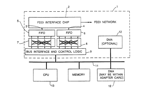
Figure 1 illustrates in schematic form an adaptor card
1, including a FDDI interface circuit 2 connected to a
computer bus 11. A PC processor (CPU) 13 and memory 15
together with optional DMA 12 are also connected to the
computer bus. The circuit 2 is of conventional form and in
this example has a 32 bit input port 3 for receiving
portions of frames to be transmitted on the network and a
32 bit output port 4 for receiving portions of frames to be
sent to the computer bus 11. Although the circuit is
described with reference to 32 bit ports in this example,
it is equally applicable to other sizes for example 16 bit
or 64 bit ports for connection to 16 or 64 bit FIFOs
respectively.
Mounted on the adapter card 1 is a 32 bit transmit
FIFO 5 coupled in use to the input port 3 and a 32 bit
receive FIFO 6 connected in use to the output port 4. Each
of the FIFOs is formed of four subsidiary FIFOs 5A-5D, 6A-
6D respectively (Figures 2 and 7), each subsidiary FIFO
being 8 bits wide (ie 1 byte)
The adapter card 1 also supports a pair of byte
alignment devices 7, 8 each having four input ports and four
output ports. Each input port is connectable with any one
of the output ports under the control of bus interface and
control logic 9 also mounted on the card 1. As can be seen
from Figure 1, therefore, on the transmit side, a byte
which is sent to the byte alignment device 7 can be routed
to any one of the four subsidiary FIFOs 5A-5D.
Correspondingly, on the receive side, the contents of any
of the subsidiary FIFOs 6A-6D can be routed to any one of
the output ports of the byte alignment device 8.
Effectively, the adapter card 1 appears as two 32 bit
mail boxes. On transmit any combination of bytes, words (2
bytes), and double words (4 bytes) can be written with any
WO 94117476 PCT/GB94/00094
.. . .
byte alignment using either the processor 13 on the PC
mothercard or a separate DMA device 12 on the adapter card
(or as part of the mothercard). The alignment logic will
ensure that the data is assembled into contiguous memory
5 within the FIFOs. On transmit typically the processor
would write the header for the protocol in use (the first
few bytes of the frame to be sent), and the DMA engine 12
write the data part on the frame into the adapter card.
There is no need to use the PC's processor 13 to assemble
all the fragments of a frame to transmit into one
contiguous block of memory.
On receive the processor 13 may read bytes, words or
double words as required by the protocol of the received
frame to decode where the remainder of the frame should
be
copied (either under processor control or by the DMA
engine).
An example of a receive operation will now be
described with reference to Figures 2 to 6. In this case,
a received FDDI frame is shown containing part of a file
being transferred under a TCP/IP protocol. The protocol
header is in three parts: FDDI, IP and TCP headers. The
size of the FDDI, IP and TCP headers has been reduced for
the purposes of this explanation. (In practice each of
these protocol headers may be up to 30 bytes long.) Each
of
these header components must be analysed in turn before
the
subsequent header layer can be decoded. The receive and
transmit FIFOs may contain more than one frame in normal
operation. Only one frame has been illustrated to simplify
the explanation.
In operation, therefore, a frame arrives on the
network at the interface circuit 2 and successive bytes
of
. the frame are supplied to successive locations in the
subsidiary FIFOs 6A-6D in sequence. Thus the first byte
of the FDDI header is supplied to the first location in
the
FIFO 6A, the second byte to the first location in the FIFO
6B, the third byte to the first location in the FIFO 6C
and
the fourth byte to the first location in the FIFO 6D.
WO 94/17476 . ' PCTIGB94/00094
2~~2~'~s
The remaining two bytes of the FDDI header are supplied to
the FIFOs 6A, 6B in sequence with the result that the
preceding bytes in the FIFOs 6A, 6B are transferred towards
the output of those FIFOs. Next, the three bytes of the
IP header are loaded in a similar fashion followed by the
five bytes of the TCP header. Following this, the
information frame which may amount to several thousand
bytes is loaded followed finally by an end byte which is
loaded into a status FIFO 10. At this stage, the memory
6 holds the information in the form shown in Figure 2.
In a second implementation, the length and status of
each received frame is written into the status FIFO 10 and
the CPU/DMA can then recover the status and length of the
received frame before processing the header.
The CPU 13 then needs to read the FDDI header. This
is achieved in a first transfer step by setting the data
alignment device 8 to connect the input ports, as shown in
Figure 2, to its output ports which are in turn connected
to the bus interface 9 such that the leading bytes in the
four FIFO 6A-6D pass through the alignment device 8 in the
same order to the interface 9. The CPU 13 then reads
these four bytes and then needs to obtain the remaining two
bytes of the FDDI header. These are obtained by loading
the two bytes which are now the leading bytes in the FIFOs
6A, 6B through the alignment device 8 in the same order
into the interface 9.
At this stage, the contents of the FIFOs 6A-6D is as
shown in Figure 3. The CPU then needs to read the IP
header. The control logic 9 will have maintained a pointer
to the next byte of data to be read from the receive memory
6 and as a result the control logic will pass the first
byte of the IP header from FIFO 6C to the bus interface 9
as shown in Figure 3 by suitably connecting the required
ports of the alignment device 8. The action of the CPU 13
in trying to read the byte causes the alignment logic to
select and read the correct byte and align it correctly on
the computer bus for the CPU. It should be noted that the
WO 94117476 PCTIGB94100094
~i~~4'~~
operation of the alignment logic is effectively "invisible"
to the CPU. The CPU simply asks for the size of data it
wishes to receive. This information is encoded in the
memory read request on the computer bus. The alignment
logic selects and aligns the correct data from the FTFO and
,, repeats the read operation, returning the requested data
to
the CPU. In this simplified example, the CPU 13 would
process the first IP byte and determine that an additional
word (2 bytes) needs to be read to complete the IP protocol
header. The CPU then issues a word read command and
receives the remainder of the IP header as shown in Figure
4. In response to this word read command, the alignment
device 8 is controlled to access the leading bytes from the
FIFOs 6D and then 6A which are passed to the computer bus
11 via the interface 9. It should be noted that no byte
masking or rotation operations have been required by the
CPU to isolate the IP header information.
The TCP header can then be read and processed in a
similar manner. For example, the CPU can read the TCP
header as a byte followed by a 32 bit double word.
At this stage, as shown in Figure 5, only the
information field remains in the memory 6. This can then
be read out by the CPU 13 or instead by the DMA 12. As can
be seen from Figure 2, the first two bytes in the
information frame are contained in the FIFOs 6C, 6D and
thus, as can be seen in Figure 5, the alignment device 8
must be set up to reverse the order of adjacent pairs of
bytes read from the FIFOs 6A-6D in each transfer step to
obtain the correct order of the information data. The 32
bit values in the interface 9 are read by the DMA
controller.
The final byte of the frame could then be read
automatically using a sophisticated DMA controller 12 or
by
- the CPU 13, this final step being shown in Figure 6.
An example of a transmit sequence will now be
described. Figure 7 illustrates the FIFO 5 in more detail
and shows an additional FIFO 14 positioned alongside. The
WO 94/17476 PCT/GB94/00094
21~~~'~~
_ s
status FIFO 14 can be'loaded with status information such
as end of frame data. Figure 7 shows the contents of the
FIFO 5 and FIFO 14 after all the data for an arbitrary
short frame has been written and before the frame is
transmitted. The data will have been written in the
following manner:
1. One byte by the processor.
2. One word (2 bytes) by the processor.
3. One longword by the processor.
4. One word by the processor.
5. Three longwords by the DMA controller.
6. End of frame marker.
Following this sequence, the FIFOs 5,14 contain the
information as shown in Figure 7. The contents of the
FIFO's 5,14 are then read out through the input port 3 onto
the FDDI network.
The loading of the FIFOs 5,14 is under the control of
the control logic 9 which maintains a record of the last
location filled and arranges for the next data to be loaded
into the next free location in the FIFO 5 by suitably
controlling the byte alignment device 7 in a similar way to
the control of the device 8.