Note : Les descriptions sont présentées dans la langue officielle dans laquelle elles ont été soumises.
End-to-end Clock Recovery for ATM Networks
This invention relates to the field of telecommunications,
and more particularly to a method and apparatus for
conveying timing information in packet switched networks,
5 such as ATM (Asynchronous Transfer Mode) networks.
In order to deliver real time interactive services, such as
voice telephony, in ATM networks, timing information must be
provided in conjunction with the payload information. This
timing information is used for the synchronization of
encoded payload at the user' s decoder/encoder_ -
The existing telephone network is a synchronous Time
Division Multiplexed (TDM) network. This digital network
(PSTN -Public Switched Telephone Network) uses 8 kHz timing
information for synchronization and delivery of real-time
15 information with a constant delay between two end points,
e . g ., a telephone conversation .
A B-ISDN (Broadband Integrated Services Digital Network)
network uses Asynchronous Transfer Mode (ATM) technology for
transport and switching . To transport real - time inf ormation
20 such as voice telephony between PSTN/PBXs synchronous
networks and B - ISDN (ATM) asynchronous networks, some means
must be provided to convey end-to-end timing in~ormation for
the encoded information.
A known method for conveying timing information makes use of
25 loop-timing. Loop-timing uses the physical layer of the
interface to encode and transport 8 kHz timing information
from the switch to the endstation. With this method the
synchronization must be extended from the narrowband TDM
PSTN or private PBX network to the ATM network. However,
-- 1 --
2~G1~2
.
most ATM premise equipment manufactured and sold today
cannot deliver 8 kHz timing information using loop-timing.
An object of the present invention is to overcome this
disadvantage .
s Accordingly the present invention provides a method of
conveying payload timing inf~w~t;nn between a source and
destin~t;~n over an asynchronous network wherein data is
transmitted packets include header and payload f ields,
comprising the steps of emitting said packets at the ~ource
10 at a rate related to the payload timing information; and
recovering said timing information at the destination from
the rate of arrival of said packets.
Preferably, said network is an ATM network, in which case
said packets are ATM cells.
15 While the method in accordance with the invention will be
described in connection with 3 . l k~z ~-Law or A-Law encoded
64 kbit/s PCM information, it i~ applicable to other data
rates and other Pn~nfling schemes. This end-to-end clock
recovery method described is transmission rate and ATM
20 Adaptation Layer (AAL) independent. It can be used for any
application and any A~L where delivery of end-to-end timing
information is required, such as, t~lPrh~ny voice, E~.320
video, encrypted data, etc.
For 64 kbit/s ~-Law or A-Law PCM encoded information, one
25 octet of PCM encoded information is transmitted (64 kbit/s)
every 125 IlS. If a cell PDU (Payload Data Unit) size of 48
octets (AAL 0) is u~ed, it would take 6 ms. For a cell PDb
size of 47 octets (AAL l) it would take 5 . 875 ms . It can be
deduced that in a constant bit rate service, a 48 o~tet PDU
30 size ~ell is received every 6 ms for the duration of the
-- 2 --
.. ., . _ . . _ _ . _
216~172
connection. For a cell PDIJ size of 47 octets, it would be
5 875 ms. Therefore, the ATM source will emit ATM cells
every 6 ms to the ATM network. For different data rates,
e g., 384 kbit/s it would be one cell per 1 ms for 48 octet
5 PDU cell size.
For 64 kbit/s data rates;
one octet every 125 ~lS = 64 kbits/s
and ATM PDU cell size = 48 octets (AAL 0)
Therefore; ATM PDU size x data transmission rate = cell
emission rate
48 x 125~s= 6 ms
For 384 kbit/s data rates, which is equivalent to 6
octets every 125 IlS
48 x 125~s/6= 1 ms
15 Below is a table showing several different data rates and
the calculated cell emission rate for cell PDU size of 48
octets ~AAL 0) .
Table 1: Cell Emission Rate for different data rates (AAL 0)
Number o~ Data Rate Cell Size Cell Emission Rate
Channels Kbit/s in Octets in msec.
64 4a 6
2 12a 4a 3
3 192 4a 2
4 256 48 l . 5
320 48 1.2
6 384 48
-- 3 --
21~1'72
8 512 48 0.75
640 48 0.6
12 768 48 O.S
960 48 0.4
16 1024 48 0.375
1280 48 0.3
24 1536 48 0.25
1600 48 0.24
1920 48 0.2
32 2048 48 0.1875
2560 48 O.lS
48 3072 48 0 . 125
S0 3200 48 0 . 12
3840 48 0.1
64 4096 48 0.09375
4800 48 0.08
5120 48 0.075
96 6144 48 0 . 0625
100 6400 48 0.06
120 7680 48 0 . 05
125 8000 48 0.048
128 8192 48 0 . 046875
For ATM PDU size of 47 octets (AAL 1) there is only one
practical data rate: 64 3~bit/s, since 47 is a primary
number. Therefore t31e cell emission rate is;
47 x 125 ~us = 5 . 875 ms
The invention also provides an alLd~ t for conveyin~
payload timing information between a ~ource and destination
-- 4 --
~16~1 ~2
. ~
over an asynchronous network wherein data is transmitted
packets include header and payload fields, comprising a
packet emitter at said ~ource for emitting packets over a
constant bit rate virtual connection through said network;
5 clock means for controlling the rate of emission of said
cells from said cell emitter with reference to the payload
timing information to be conveyed; a cell receiver at the
destination ~or receiving said cells from the network; and a
payload clock recovering said timing information at the
10 destination from the rate of arrival of in~ ming cells.
The invention will now be described in more detail, by way
of example only, with reference to the accompanying
drawings, in which:
Figure l is a block diagram of a system in accordance with
5 the inventioni
Figure 2 shows an ATM cell header format (UNI);
Figure 3 shows cell flow in an ATM CBR connection;
Figure 4 is a ~lock diagram of a clock control and filter
circuit; and
20 Figure 5 is a timing diagram showing ~TcO tracking of
received cell emission rate.
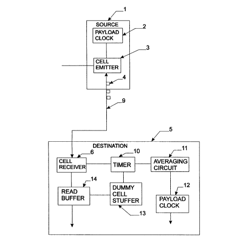
Referring to Figure l, a source I is connected to a
destination 5 via a virtual connection established through
an ATM network in a conventional manner.
25 Source 1 i n~ a cell emitter 3 that emit~ ATM cells 4
over a constant bit rate, virtual connection at a rate that
is related to payload clock 2, which references the timing
information for the payload data of the ATM cells 4.
-- 5
216~72
At the destination 5, the ATM cells 4 are received by cell
receiver 6, which transfers the cells to read buffer 14.
The rate of arrival of cells is timed by timer 10 and
averaged by averaging circuit 11. Destination payload clock
s 12 generates payload clock signals referenced to the average
rate of arrival of cells at cell receiver 6.
Thus, it will be seen that the cell emission rate of the
virtual connection (VC) is used to convey the timing
information for a constant bit rate (CBR) ATM con~ection
10 between the source 1 and the destination 5. The timer 10 is
also used to detect lost or severely delayed cells because
the ATM network has a low probability that cells may be lost
or delayed due to switch congestion or bit errors.
At the desination 5, the clock rate is adjusted to determine
15 how quickly the received information will be read out from
the receive buf f er 14 . The rate of reading inf ormation f rom
the buf f er must equal the rate of inf ormation being written
into the buffer. If this relationship can be m:~;nt;~ln~
there will be no over-run or under-run of the receive
20 buf f er .
Each cell 4 that is transmitted f rom the cell emitter 3 has
a five octet header. The header is used for routing of the
cell in ATM switches. Figure 2 is a diagram of cell header
format. The fifth octet of the header is called "Header
2s Error Control" (HEC). It is used for detection/correction of
bit errors in the ATM cell header. This HEC octet is used to
convey the cell e_ission rate o~ the transmitter over the
Virtual Connection (VC).
The properties of the ATM network are such that the network
30 will introduce a cell delay variation (CDV) or jitter for
-- 6 --
~, 216~17~
any CBR connection. Also, cells can be lost or severely
delayed (greater than CDV of the VC~ in the network.
Therefore, the method must be able to convey timing
information under the above conditions.
5 First it must be determined when an ATM cell is lost or
severely delayed. This is accomplished by using the timer 10
~Timer_A in Figure 3 ) that times the arrival interval
between cells. The reception of a "~eader Error Controla
~HEC) octet in the VC that requires timing information to be
10 conveyed is used to trigger Timer_A. ~nder normal
conditions, a 48 octet PDU cell size will arrive every 6 ms.
for 64 kbit/s service. The maximum CDV of the ATM network
will be determined using signaling and added to the total
delay. For this example a CDV of 2 ms maximum will be used.
15 There~ore, Timer 10 is set to PDU cell segmentation delay
plus the maximum CDV o~ the network connection; 6 ms + 2 ms
= 8 ms.
The expiration of Timer_A indicates that a cell has not
arrived for the virtual channel in question within the time
20 allowed ~8 ms), and there~ore the cell is lost or severely
delayed. A severely delayed cell is a cell that has a longer
delay than what was negotiated by signaling at the beginning
of the connection. For one or more cells that are lost or
not delivered in time, one or more dummy cells C~ntil;n;ng
25 silence information are to the payload for voice
connections. This keeps the buf~er at the right level ~no
underflow) . Also the system keeps track of how many dummy
cells were added.
Figure 3 shows cells being packaged and transmitted at f ixed
30 time intervals, every 6 ms. At the destination, it shows
-- 7 --
,~ 2~ 2
that cells arriving at the receiver with some CDV (Cell
Delay Variation). In this example, cell n+2 was lost in the
ATM network. A dummy cell was added to mA;ntA;n proper
information flow from the buffer to the decoder. This
S locally generated dummy cell is of the same frequency and
phase as the locally generated cell emission rate pulse.
Therefore there is no VCO clock adjustment on the insertion
of a dummy cell.
At the source, the cell emission clock is referenced to the
information encoder (payload) clock 2. Therefore the
transmitter' s encoding clock can be recovered at destination
by dPtPrm;n;nr~ the rate of arrival of incoming cells. Any
cell that is not delivered must be substituted with dummy
silence cell so that the decoder will receives cell every 6
ms or an octet every 125 lls.
The ATM networ]{ delivers the payload (cells) with jitter
(CDV) of 2 ms in this example . This cell reception j itter
needs to be filtered. Figure 4 shows a simplified block
diagram of Digital Frer~ency/Phase Detector which will
determine if the receive payload clock 12 is running slow or
fast. This detector compares the phases of the two clocks
and decides if the frequency (fx) of the VCO needs to be
increased or decreased.
The circuit for Pl~tr~rtin~ the clock signals from the
2s incoming cells is shown in more detail in Figure 4. Digital
freo~uency and phase detector 20 receives at its inputs the
incoming cell arrival rate and the generated clock f requency
fx at the dest;n~t;on 5. The detector 20 generates
respective down or up pulses connected through tri-statable
buffers 21, 22 to integrator 23 whose output is connected to
-- 8
_ _ _ _ _ _ _ _ _ _ . , .. .. .. . . . _ ..... _ . .
9 1 12
voltage controlled oscillator 24 generating the recovered
clock signal fx~ This signal fx is the applied through
divider 25 as the feedback signal to the second input of the
detector 20.
s Figure 5 is a timing diagram showing the two clock rates and
how the digital frequency/phase detector generates pulses to
the integrator 13 for adjustment of the frequency of VCO 14. -
The purpose of the integrator 23 is to control the rate of
change of output frequency the VCO 24. The integrator 23 can
10 change the voltage thre~hold to the VCO 24. The rate of
voltage change to the integrator 23 is programmed by
resistor Rl and capacitor C1. The duration of the change is
controlled by the width of "Upr/ or "Down" pulses output by
the detector 20. If there is no pulse from the digital
1~ Fre~uency/Pha~e Detector, the integrator will produce a
constant voltage level to the VCO 14, which will hold its
f requency .
The descrlbed end-to-end clock recovery method can convey
timing information over asynchronous ATM networks without
20 the need of 8 k~z frame information being encoded into the
physical interfaces. The described method works over current
ATM networks and does not require any additional bandwidth
or control information from the ATM network. The method is
transparent to the ATM network.
_ g _